- 您現(xiàn)在的位置:買賣IC網 > PDF目錄373631 > TFRA08C13 (Lineage Power) Ultraframer DS3/E3/DS2/E2/DS1/E1/DS0 PDF資料下載
參數(shù)資料
| 型號: | TFRA08C13 |
| 廠商: | Lineage Power |
| 元件分類: | 通信及網絡 |
| 英文描述: | Ultraframer DS3/E3/DS2/E2/DS1/E1/DS0 |
| 中文描述: | Ultraframer DS3/E3/DS2/E2/DS1/E1/DS0 |
| 文件頁數(shù): | 127/188頁 |
| 文件大小: | 3047K |
| 代理商: | TFRA08C13 |
第1頁第2頁第3頁第4頁第5頁第6頁第7頁第8頁第9頁第10頁第11頁第12頁第13頁第14頁第15頁第16頁第17頁第18頁第19頁第20頁第21頁第22頁第23頁第24頁第25頁第26頁第27頁第28頁第29頁第30頁第31頁第32頁第33頁第34頁第35頁第36頁第37頁第38頁第39頁第40頁第41頁第42頁第43頁第44頁第45頁第46頁第47頁第48頁第49頁第50頁第51頁第52頁第53頁第54頁第55頁第56頁第57頁第58頁第59頁第60頁第61頁第62頁第63頁第64頁第65頁第66頁第67頁第68頁第69頁第70頁第71頁第72頁第73頁第74頁第75頁第76頁第77頁第78頁第79頁第80頁第81頁第82頁第83頁第84頁第85頁第86頁第87頁第88頁第89頁第90頁第91頁第92頁第93頁第94頁第95頁第96頁第97頁第98頁第99頁第100頁第101頁第102頁第103頁第104頁第105頁第106頁第107頁第108頁第109頁第110頁第111頁第112頁第113頁第114頁第115頁第116頁第117頁第118頁第119頁第120頁第121頁第122頁第123頁第124頁第125頁第126頁當前第127頁第128頁第129頁第130頁第131頁第132頁第133頁第134頁第135頁第136頁第137頁第138頁第139頁第140頁第141頁第142頁第143頁第144頁第145頁第146頁第147頁第148頁第149頁第150頁第151頁第152頁第153頁第154頁第155頁第156頁第157頁第158頁第159頁第160頁第161頁第162頁第163頁第164頁第165頁第166頁第167頁第168頁第169頁第170頁第171頁第172頁第173頁第174頁第175頁第176頁第177頁第178頁第179頁第180頁第181頁第182頁第183頁第184頁第185頁第186頁第187頁第188頁
Lucent Technologies Inc.
127
Preliminary Data Sheet
October 2000
TFRA08C13 OCTAL T1/E1 Framer
Global Register Structure
(continued)
Global PLLCK Control Register (GREG9)
This register selectively enables/disables an individual transmit framer’s internal clock synthesizer. setting all bits to
0 (the default condition) disables all transmit framer clock synthesizers, and allows an external source of PLLCK to
drive the transmit framers.
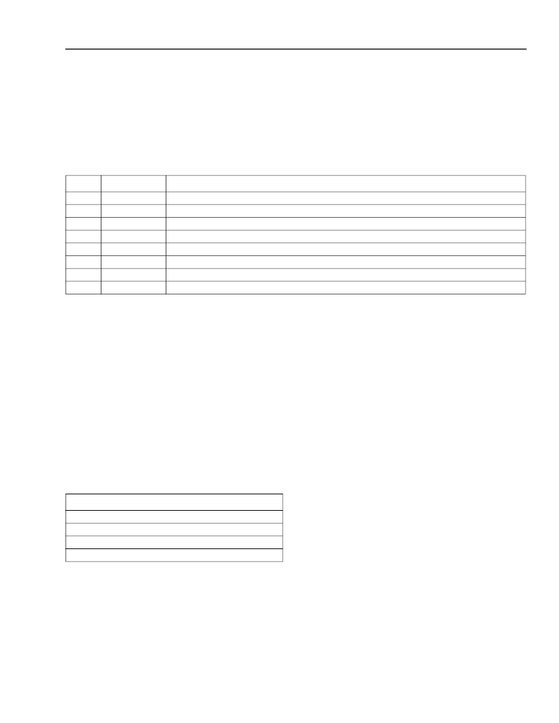
Table 67. Global PLLCK Control Register (GREG9) (009)
Bit
0
1
2
3
4
5
6
7
Symbol
EIPLLCK1
EIPLLCK2
EIPLLCK3
EIPLLCK4
EIPLLCK5
EIPLLCK6
EIPLLCK7
EIPLLCK8
Description
Enable Transmit Framer 1’s Internal PLLCK Clock Synthesizer.
Enable Transmit Framer 2’s Internal PLLCK Clock Synthesizer.
Enable Transmit Framer 3’s Internal PLLCK Clock Synthesizer.
Enable Transmit Framer 4’s Internal PLLCK Clock Synthesizer.
Enable Transmit Framer 5’s Internal PLLCK Clock Synthesizer.
Enable Transmit Framer 6’s Internal PLLCK Clock Synthesizer.
Enable Transmit Framer 7’s Internal PLLCK Clock Synthesizer.
Enable Transmit Framer 8’s Internal PLLCK Clock Synthesizer.
Framer Register Architecture
REGBANK1—REGBANK8 contain the status and pro-
grammable control registers for the framer and system
CHI interface channels FRM1—FRM8. The base
address for REGBANK1—REGBANK8 is Y00 (hex),
where Y = 2—9 for FRM1—FRM8, respectively. Within
these register banks, the bit map is identical for
FRM1—FRM8.
The framer registers are structures as shown in Table
68. Default values are given in the individual register
definition tables.
Table 68. Framer Status and Control Blocks
Address Range (Hexadecimal)
* The most significant digit, designated by Y, is used to identify each
framer (for framer 1—framer 8, Y = 2—9, respectively).
The complete register map for the framer is given in
Table 182—Table 186. The address of the registers is
shown in the table title with the most significant digit,
designated by Y, used to identify each framer (for
framer 1—framer 8, Y = 2—9, respectively).
All status registers are clocked with the internal framer
receive line clock (RFRMCK).
Bits in status registers FRM_SR1 and FRM_SR7 are
set at the onset of the condition and are cleared on
read when the given condition is no longer present.
These registers can generate interrupts if the corre-
sponding register bits are enabled in interrupt enable
registers FRM_PR0—FRM_PR7.
On all 16-bit counter registers (FRM_SR8—
FRM_SR51), both bytes are cleared only after reading
both bytes. These status registers are two byte register
pairs. These register pairs must be read in succession,
with the lower byte read first followed by a read of
higher byte. Once a read is initiated on one of the
bytes, the updating of that counter is disabled and
remains disabled until both bytes are read. All events
during this interval are lost. Updating of the counter
registers is stopped when all of the bits are set to 1.
Updating resumes after the registers are cleared on
read. These register pairs may be read in any order,
but they must be read in pairs, i.e., a read of 1 byte
must be followed immediately by a read of the remain-
ing byte of the pair.
Status registers FRM_SR0—FRM_SR63 are clear-on-
read (COR) registers. These registers are cleared by
the framer internal received line clock (RFRMCK). At
least two RFRMCK cycles (1.3 μs for DS1 and 1.0 μs
for CEPT) must be allowed between successive reads
of the same COR register to allow it to properly clear.
Framer Register Block
Status Registers (COR) (Y00—Y3F)*
Receive Signaling Registers (Y40—Y5F)*
Parameter (Configuration) Registers (Y60—YA6)*
Transmit Signaling Registers (YE0—YFF)*
相關PDF資料 |
PDF描述 |
|---|---|
| TFS380C | VI TELEFILTER Filter specification |
| TFT0675F | Anti-Aliasing and Reconstruction TFT range |
| TFT0675S | Anti-Aliasing and Reconstruction TFT range |
| TFT1350F | Anti-Aliasing and Reconstruction TFT range |
| TFT1350S | Anti-Aliasing and Reconstruction TFT range |
相關代理商/技術參數(shù) |
參數(shù)描述 |
|---|---|
| TFRA08C13-DB | 制造商:AGERE 制造商全稱:AGERE 功能描述:TFRA08C13 OCTAL T1/E1 Framer |
| TFRA28J133BAL-1 | 制造商:未知廠家 制造商全稱:未知廠家 功能描述:Telecomm/Datacomm |
| TFRA84J13 | 制造商:AGERE 制造商全稱:AGERE 功能描述:Ultraframer DS3/E3/DS2/E2/DS1/E1/DS0 |
| TFRA84J131BL-3-DB | 制造商:LSI Corporation 功能描述:Framer DS0/DS1/DS2/DS3/E1/E2/E3 1.5V/3.3V 909-Pin BGA |
| TFRA84J13DS0 | 制造商:AGERE 制造商全稱:AGERE 功能描述:Ultraframer DS3/E3/DS2/E2/DS1/E1/DS0 |
發(fā)布緊急采購,3分鐘左右您將得到回復。