- 您現(xiàn)在的位置:買(mǎi)賣(mài)IC網(wǎng) > PDF目錄373631 > TFRA08C13 (Lineage Power) Ultraframer DS3/E3/DS2/E2/DS1/E1/DS0 PDF資料下載
參數(shù)資料
| 型號(hào): | TFRA08C13 |
| 廠商: | Lineage Power |
| 元件分類(lèi): | 通信及網(wǎng)絡(luò) |
| 英文描述: | Ultraframer DS3/E3/DS2/E2/DS1/E1/DS0 |
| 中文描述: | Ultraframer DS3/E3/DS2/E2/DS1/E1/DS0 |
| 文件頁(yè)數(shù): | 96/188頁(yè) |
| 文件大?。?/td> | 3047K |
| 代理商: | TFRA08C13 |
第1頁(yè)第2頁(yè)第3頁(yè)第4頁(yè)第5頁(yè)第6頁(yè)第7頁(yè)第8頁(yè)第9頁(yè)第10頁(yè)第11頁(yè)第12頁(yè)第13頁(yè)第14頁(yè)第15頁(yè)第16頁(yè)第17頁(yè)第18頁(yè)第19頁(yè)第20頁(yè)第21頁(yè)第22頁(yè)第23頁(yè)第24頁(yè)第25頁(yè)第26頁(yè)第27頁(yè)第28頁(yè)第29頁(yè)第30頁(yè)第31頁(yè)第32頁(yè)第33頁(yè)第34頁(yè)第35頁(yè)第36頁(yè)第37頁(yè)第38頁(yè)第39頁(yè)第40頁(yè)第41頁(yè)第42頁(yè)第43頁(yè)第44頁(yè)第45頁(yè)第46頁(yè)第47頁(yè)第48頁(yè)第49頁(yè)第50頁(yè)第51頁(yè)第52頁(yè)第53頁(yè)第54頁(yè)第55頁(yè)第56頁(yè)第57頁(yè)第58頁(yè)第59頁(yè)第60頁(yè)第61頁(yè)第62頁(yè)第63頁(yè)第64頁(yè)第65頁(yè)第66頁(yè)第67頁(yè)第68頁(yè)第69頁(yè)第70頁(yè)第71頁(yè)第72頁(yè)第73頁(yè)第74頁(yè)第75頁(yè)第76頁(yè)第77頁(yè)第78頁(yè)第79頁(yè)第80頁(yè)第81頁(yè)第82頁(yè)第83頁(yè)第84頁(yè)第85頁(yè)第86頁(yè)第87頁(yè)第88頁(yè)第89頁(yè)第90頁(yè)第91頁(yè)第92頁(yè)第93頁(yè)第94頁(yè)第95頁(yè)當(dāng)前第96頁(yè)第97頁(yè)第98頁(yè)第99頁(yè)第100頁(yè)第101頁(yè)第102頁(yè)第103頁(yè)第104頁(yè)第105頁(yè)第106頁(yè)第107頁(yè)第108頁(yè)第109頁(yè)第110頁(yè)第111頁(yè)第112頁(yè)第113頁(yè)第114頁(yè)第115頁(yè)第116頁(yè)第117頁(yè)第118頁(yè)第119頁(yè)第120頁(yè)第121頁(yè)第122頁(yè)第123頁(yè)第124頁(yè)第125頁(yè)第126頁(yè)第127頁(yè)第128頁(yè)第129頁(yè)第130頁(yè)第131頁(yè)第132頁(yè)第133頁(yè)第134頁(yè)第135頁(yè)第136頁(yè)第137頁(yè)第138頁(yè)第139頁(yè)第140頁(yè)第141頁(yè)第142頁(yè)第143頁(yè)第144頁(yè)第145頁(yè)第146頁(yè)第147頁(yè)第148頁(yè)第149頁(yè)第150頁(yè)第151頁(yè)第152頁(yè)第153頁(yè)第154頁(yè)第155頁(yè)第156頁(yè)第157頁(yè)第158頁(yè)第159頁(yè)第160頁(yè)第161頁(yè)第162頁(yè)第163頁(yè)第164頁(yè)第165頁(yè)第166頁(yè)第167頁(yè)第168頁(yè)第169頁(yè)第170頁(yè)第171頁(yè)第172頁(yè)第173頁(yè)第174頁(yè)第175頁(yè)第176頁(yè)第177頁(yè)第178頁(yè)第179頁(yè)第180頁(yè)第181頁(yè)第182頁(yè)第183頁(yè)第184頁(yè)第185頁(yè)第186頁(yè)第187頁(yè)第188頁(yè)
96
LLucent Technologies Inc.
Preliminary Data Sheet
October 2000
TFRA08C13 OCTAL T1/E1 Framer
Facility Data Link
(continued)
5-4563(F)r.1
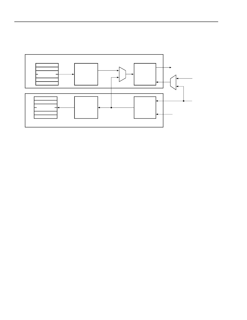
Figure 35. Remote Loopback Mode
XMIT HDLC FDL BLOCK
XMIT HDLC
FDL XMIT
INTERFACE
XMIT FIFO
RCVR FIFO
RCVR HDLC
FDL RCVR
INTERFACE
TFDL
TFDLCK
RFDLCK
RFDL
RCVR HDLC FDL BLOCK
Phase-Lock Loop Circuit
The TFRA08C13 allows for independent transmit path
and receive path clocking. The device provides outputs
to control variable clock oscillators on both the transmit
and receive paths. As such, the system may have both
the transmit and receive paths phase-locked to two
autonomous clock sources.
The block diagram of the TFRA08C13 phase detector
circuitry is shown in Figure 36. The TFRA08C13 uses
elastic store buffers (two frames) to accommodate the
transfer of data from the system interface clock rate of
2.048 Mbits/s to the line interface clock rate of either
1.544 Mbits/s or 2.048 Mbits/s. The transmit line side of
the TFRA08C13 does not have any mechanism to
monitor data overruns or underruns (slips) in its elastic
store buffer. This interface relies on the requirement
that the PLLCK clock signal (variable) is phase-locked
to the CHICK clock signal (reference). When this
requirement is not met, uncontrolled slips may occur in
the transmit elastic store buffer that would result in cor-
rupting data and no indication will be given. Typically, a
variable clock oscillator (VCXO) is used to drive the
PLLCK signal. The TFRA08C13 provides a phase error
signal (PLLCK-EPLL) that can be used to control the
VCXO PLLCK. The PLLCK-EPLL signal is generated
by monitoring the divided-down PLLCK (DIV-PLLCK)
and CHICK (DIV-CHICK) signals. The DIV-CHICK sig-
nal is used as the reference to determine the phase dif-
ference between DIV-CHICK and DIV-PLLCK. While
DIV-CHICK and DIVPLLCK are phase-locked, the
PLLCK-EPLL signal is in a high-impedance state. A
phase difference between DIV-CHICK and DIV-PLLCK
drives PLLCK-EPLL to either 3.3 V or 0 V. An appropri-
ate loop filter, for example, an RC circuit with R = 1 k
and C = 0.1 μF, is used to filter these PLLCK-EPLL
pulses to control the VCXO.
The system can force CHICK to be phase-locked to
RLCK by using RLCK as a reference signal to control a
VCXO that is sourcing the CHICK signal. The
TFRA08C13 uses the receive line signal (RLCK) as the
reference and the CHICK signal as the variable signal.
The TFRA08C13 provides a phase error signal
(CHICK-EPLL) that can be used to control the VCXO
generating CHICK. The CHICK-EPLL signal is gener-
ated by monitoring the divided-down CHICK signal
(DIV-CHICK) and RLCK (DIV-RLCK) signals. The DIV-
RLCK signal is used as the reference to determine the
phase difference between DIV-CHICK and DIV-RLCK.
While DIV-RLCK and DIV-CHICK are phase-locked, the
CHICK-EPLL signal is in a high-impedance state. A
phase difference between DIV-RLCK and DIV-CHICK
drives CHICK-EPLL to either 3.3 V or 0 V. An appropri-
ate loop filter, for example, an RC circuit with R = 1 k
and C = 0.1 μF, is used to filter these CHICK-EPLL
pulses to control the VCXO. In this mode, the
TFRA08C13 can be programmed to act as a master
timing source and is capable of generating the system
frame synchronization signal through the CHIFS pin
and setting FRM_PR45 bit 4 to 1.
相關(guān)PDF資料 |
PDF描述 |
|---|---|
| TFS380C | VI TELEFILTER Filter specification |
| TFT0675F | Anti-Aliasing and Reconstruction TFT range |
| TFT0675S | Anti-Aliasing and Reconstruction TFT range |
| TFT1350F | Anti-Aliasing and Reconstruction TFT range |
| TFT1350S | Anti-Aliasing and Reconstruction TFT range |
相關(guān)代理商/技術(shù)參數(shù) |
參數(shù)描述 |
|---|---|
| TFRA08C13-DB | 制造商:AGERE 制造商全稱(chēng):AGERE 功能描述:TFRA08C13 OCTAL T1/E1 Framer |
| TFRA28J133BAL-1 | 制造商:未知廠家 制造商全稱(chēng):未知廠家 功能描述:Telecomm/Datacomm |
| TFRA84J13 | 制造商:AGERE 制造商全稱(chēng):AGERE 功能描述:Ultraframer DS3/E3/DS2/E2/DS1/E1/DS0 |
| TFRA84J131BL-3-DB | 制造商:LSI Corporation 功能描述:Framer DS0/DS1/DS2/DS3/E1/E2/E3 1.5V/3.3V 909-Pin BGA |
| TFRA84J13DS0 | 制造商:AGERE 制造商全稱(chēng):AGERE 功能描述:Ultraframer DS3/E3/DS2/E2/DS1/E1/DS0 |
發(fā)布緊急采購(gòu),3分鐘左右您將得到回復(fù)。