- 您現(xiàn)在的位置:買賣IC網(wǎng) > PDF目錄383961 > TMX320DM6443AZWT (Texas Instruments, Inc.) Digital Media System-on-Chip PDF資料下載
參數(shù)資料
| 型號: | TMX320DM6443AZWT |
| 廠商: | Texas Instruments, Inc. |
| 英文描述: | Digital Media System-on-Chip |
| 中文描述: | 數(shù)字媒體系統(tǒng)片上 |
| 文件頁數(shù): | 19/221頁 |
| 文件大?。?/td> | 1582K |
| 代理商: | TMX320DM6443AZWT |
第1頁第2頁第3頁第4頁第5頁第6頁第7頁第8頁第9頁第10頁第11頁第12頁第13頁第14頁第15頁第16頁第17頁第18頁當(dāng)前第19頁第20頁第21頁第22頁第23頁第24頁第25頁第26頁第27頁第28頁第29頁第30頁第31頁第32頁第33頁第34頁第35頁第36頁第37頁第38頁第39頁第40頁第41頁第42頁第43頁第44頁第45頁第46頁第47頁第48頁第49頁第50頁第51頁第52頁第53頁第54頁第55頁第56頁第57頁第58頁第59頁第60頁第61頁第62頁第63頁第64頁第65頁第66頁第67頁第68頁第69頁第70頁第71頁第72頁第73頁第74頁第75頁第76頁第77頁第78頁第79頁第80頁第81頁第82頁第83頁第84頁第85頁第86頁第87頁第88頁第89頁第90頁第91頁第92頁第93頁第94頁第95頁第96頁第97頁第98頁第99頁第100頁第101頁第102頁第103頁第104頁第105頁第106頁第107頁第108頁第109頁第110頁第111頁第112頁第113頁第114頁第115頁第116頁第117頁第118頁第119頁第120頁第121頁第122頁第123頁第124頁第125頁第126頁第127頁第128頁第129頁第130頁第131頁第132頁第133頁第134頁第135頁第136頁第137頁第138頁第139頁第140頁第141頁第142頁第143頁第144頁第145頁第146頁第147頁第148頁第149頁第150頁第151頁第152頁第153頁第154頁第155頁第156頁第157頁第158頁第159頁第160頁第161頁第162頁第163頁第164頁第165頁第166頁第167頁第168頁第169頁第170頁第171頁第172頁第173頁第174頁第175頁第176頁第177頁第178頁第179頁第180頁第181頁第182頁第183頁第184頁第185頁第186頁第187頁第188頁第189頁第190頁第191頁第192頁第193頁第194頁第195頁第196頁第197頁第198頁第199頁第200頁第201頁第202頁第203頁第204頁第205頁第206頁第207頁第208頁第209頁第210頁第211頁第212頁第213頁第214頁第215頁第216頁第217頁第218頁第219頁第220頁第221頁
www.ti.com
2.4.3
Peripherals
2.4.4
DSP Interrupt Controller
2.5 Memory Map Summary
TMS320DM6443
Digital Media System-on-Chip
SPRS282E–DECEMBER 2005–REVISED MARCH 2007
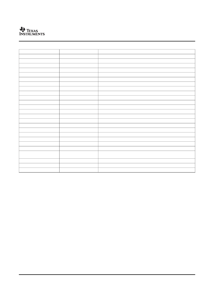
Table 2-2. C64x+ Cache Registers (continued)
HEX ADDRESS RANGE
0x0184 4034
0x0184 4038
0x0184 4040
0x0184 4044
0x0184 4048
0x0184 404C
0x0184 4050 - 0x0184 4FFF
0x0184 5000
0x0184 5004
0x0184 5008
0x0184 500C - 0x0184 5027
0x0184 5028
0x0184 502C - 0x0184 5039
0x0184 5040
0x0184 5044
0x0184 5048
0x0184 8000 - 0x0184 8004
0x0184 8008 - 0x0184 8024
0x0184 8028 - 0x0184 802C
0x0184 8030 - 0x0184 803C
0x0184 8040 - 0x0184 8104
REGISTER ACRONYM
L1DWIWC
-
L1DWBAR
L1DWWC
L1DIBAR
L1DIWC
-
L2WB
L2WBINV
L2INV
-
L1PINV
-
L1DWB
L1DWBINV
L1DINV
MAR0 - MAR1
MAR2 - MAR9
MAR10 - MAR11
MAR12 - MAR15
MAR16 - MAR65
DESCRIPTION
L1D writeback invalidate word count register
Reserved
L1D Block Writeback
L1D Block Writeback
L1D invalidate base address register
L1D invalidate word count register
Reserved
L2 writeback all register
L2 writeback invalidate all register
L2 Global Invalidate without writeback
Reserved
L1P Global Invalidate
Reserved
L1D Global Writeback
L1D Global Writeback with Invalidate
L1D Global Invalidate without writeback
Reserved 0x0000 0000 - 0x01FF FFFF
Memory Attribute Registers for EMIFA 0x0200 0000 - 0x09FF FFFF
Reserved 0x0A00 0000 - 0x0BFF FFFF
Memory Attribute Registers for VLYNQ 0x0C00 0000 - 0x0FFF FFFF
Reserved 0x1000 0000 - 0x41FF FFFF
Memory Attribute Registers for EMIFA/VLYNQ Shadow 0x4200 0000 -
0x4FFF FFFF
Reserved 0x5000 0000 - 0x7FFF FFFF
Memory Attribute Registers for DDR2 0x8000 0000 - 0x8FFF FFFF
Reserved 0x9000 0000 - 0xFFFF FFFF
0x0184 8108 - 0x0184 813C
MAR66 - MAR79
0x0184 8140- 0x0184 81FC
0x0184 8200 - 0x0184 823C
0x0184 8240 - 0x0184 83FC
MAR80 - MAR127
MAR128 - MAR143
MAR144 - MAR255
The DSP has controllability for the following peripherals:
EDMA
ASP
2 Timers (Timer0 and Timer1) that can each be configured as 1 64-bit or 2 32-bit timers
The DSP Interrupt Controller accepts device interrupts and appropriately maps them to the DSP’s
available interrupts. The DSP Interrupt Controller is briefly described in this document in the Interrupts
section. For more detailed on the DSP Interrupt Controller, see the Documentation Support section of this
document for the C64x+ CPU User's Guide.
Table 2-3
shows the memory map address ranges of the device.
Table 2-4
depicts the expanded map of
the Configuration Space (0x0180 0000 through 0x0FFF FFFF). The device has multiple on-chip memories
associated with its two processors and various subsystems. To help simplify software development a
unified memory map is used where possible to maintain a consistent view of device resources across all
bus masters.
Submit Documentation Feedback
Device Overview
19
相關(guān)PDF資料 |
PDF描述 |
|---|---|
| TMX320DM6443ZWT | Digital Media System-on-Chip |
| TMS320DM647_08 | Digital Media Processor |
| TMS320DM647ZUT720 | Digital Media Processor |
| TMS320DM647ZUT900 | Digital Media Processor |
| TMS320DM648ZUT720 | Digital Media Processor |
相關(guān)代理商/技術(shù)參數(shù) |
參數(shù)描述 |
|---|---|
| TMX320DM6443BZWT | 制造商:Texas Instruments 功能描述: |
| TMX320DM6443CZWT | 制造商:Texas Instruments 功能描述: |
| TMX320DM6443ZWT | 制造商:Texas Instruments 功能描述: |
| TMX320DM6444AZWT | 制造商:Texas Instruments 功能描述:TMS320DM6443, TMS320DM6444 DIGITAL MEDIA SOC DATA SHEET - Trays |
| TMX320DM6446AZWT | 制造商:Texas Instruments 功能描述: |
發(fā)布緊急采購,3分鐘左右您將得到回復(fù)。