- 您現(xiàn)在的位置:買(mǎi)賣(mài)IC網(wǎng) > PDF目錄372925 > XPC755BRX400LE Microprocessor PDF資料下載
參數(shù)資料
| 型號(hào): | XPC755BRX400LE |
| 英文描述: | Microprocessor |
| 中文描述: | 微處理器 |
| 文件頁(yè)數(shù): | 26/52頁(yè) |
| 文件大小: | 1274K |
| 代理商: | XPC755BRX400LE |
第1頁(yè)第2頁(yè)第3頁(yè)第4頁(yè)第5頁(yè)第6頁(yè)第7頁(yè)第8頁(yè)第9頁(yè)第10頁(yè)第11頁(yè)第12頁(yè)第13頁(yè)第14頁(yè)第15頁(yè)第16頁(yè)第17頁(yè)第18頁(yè)第19頁(yè)第20頁(yè)第21頁(yè)第22頁(yè)第23頁(yè)第24頁(yè)第25頁(yè)當(dāng)前第26頁(yè)第27頁(yè)第28頁(yè)第29頁(yè)第30頁(yè)第31頁(yè)第32頁(yè)第33頁(yè)第34頁(yè)第35頁(yè)第36頁(yè)第37頁(yè)第38頁(yè)第39頁(yè)第40頁(yè)第41頁(yè)第42頁(yè)第43頁(yè)第44頁(yè)第45頁(yè)第46頁(yè)第47頁(yè)第48頁(yè)第49頁(yè)第50頁(yè)第51頁(yè)第52頁(yè)
26
MPC755 RISC Microprocessor Hardware Specifications
MOTOROLA
Pinout Listings
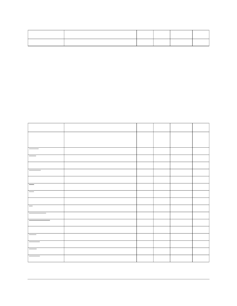
Table 15 provides the pinout listing for the MPC755, 360 PBGA and CBGA packages.
VOLTDET
F3
High
Output
—
6
Notes:
1. OV
DD
supplies power to the processor bus, JTAG, and all control signals; and V
DD
supplies power to the
processor core and the PLL (after filtering to become AV
DD
). These columns serve as a reference for the nominal
voltage supported on a given signal as selected by the BVSEL pin configuration of Table 2 and the voltage
supplied. For actual recommended value of V
in
or supply voltages, see Table 3.
2. These are test signals for factory use only and must be pulled up to OV
DD
for normal machine operation.
3. This pin must be pulled up to OV
DD
for proper operation of the processor interface. To allow for future I/O voltage
changes, provide the option to connect BVSEL independently to either OV
DD
or GND.
4. Uses 1 of 15 existing no connects in MPC740, 255 BGA package.
5. Internal pull-up on die.
6. Internally tied to GND in the MPC745, 255 BGA package to indicate to the power supply that a low-voltage
processor is present. This signal is not a power supply input.
Caution:
This differs from the MPC755, 360 BGA package.
Table 15. Pinout Listing for the MPC755, 360 BGA Package
Signal Name
Pin Number
Active
I/O
I/F Voltage
1
Notes
A[0:31]
A13, D2, H11, C1, B13, F2, C13, E5, D13, G7,
F12, G3, G6, H2, E2, L3, G5, L4, G4, J4, H7,
E1, G2, F3, J7, M3, H3, J2, J6, K3, K2, L2
High
I/O
OV
DD
AACK
N3
Low
Input
OV
DD
ABB
L7
Low
I/O
OV
DD
AP[0:3]
C4, C5, C6, C7
High
I/O
OV
DD
ARTRY
L6
Low
I/O
OV
DD
AV
DD
A8
—
—
2.0 V
BG
H1
Low
Input
OV
DD
BR
E7
Low
Output
OV
DD
BVSEL
W1
High
Input
OV
DD
3, 5, 6
CI
C2
Low
Output
OV
DD
CKSTP_IN
B8
Low
Input
OV
DD
CKSTP_OUT
D7
Low
Output
OV
DD
CLK_OUT
E3
—
Output
OV
DD
DBB
K5
Low
I/O
OV
DD
DBDIS
G1
Low
Input
OV
DD
DBG
K1
Low
Input
OV
DD
DBWO
D1
Low
Input
OV
DD
Table 14. Pinout Listing for the MPC745, 255 PBGA Package (continued)
Signal Name
Pin Number
Active
I/O
I/F Voltage
1
Notes
相關(guān)PDF資料 |
PDF描述 |
|---|---|
| XPC750EC | XPC750P/D XPC750P RISC Microprocessor Hardware Specifications |
| XPC801ZP25 | Microprocessor |
| XPC801ZP40 | Microprocessor |
| XPC821ZP40 | Microprocessor |
| XPC823ZP25 | Microprocessor |
相關(guān)代理商/技術(shù)參數(shù) |
參數(shù)描述 |
|---|---|
| XPC801ZP25 | 制造商:未知廠家 制造商全稱(chēng):未知廠家 功能描述:Microprocessor |
| XPC801ZP40 | 制造商:未知廠家 制造商全稱(chēng):未知廠家 功能描述:Microprocessor |
| XPC821ZP40 | 制造商:未知廠家 制造商全稱(chēng):未知廠家 功能描述:Microprocessor |
| XPC823CVR66B2T | 功能描述:IC MPU POWERQUICC 66MHZ 256-PBGA RoHS:是 類(lèi)別:集成電路 (IC) >> 嵌入式 - 微處理器 系列:MPC8xx 標(biāo)準(zhǔn)包裝:2 系列:MPC8xx 處理器類(lèi)型:32-位 MPC8xx PowerQUICC 特點(diǎn):- 速度:133MHz 電壓:3.3V 安裝類(lèi)型:表面貼裝 封裝/外殼:357-BBGA 供應(yīng)商設(shè)備封裝:357-PBGA(25x25) 包裝:托盤(pán) |
| XPC823CZC66A | 制造商:Freescale Semiconductor 功能描述: |
發(fā)布緊急采購(gòu),3分鐘左右您將得到回復(fù)。