- 您現(xiàn)在的位置:買賣IC網(wǎng) > PDF目錄372925 > XPC755BRX400LE Microprocessor PDF資料下載
參數(shù)資料
| 型號: | XPC755BRX400LE |
| 英文描述: | Microprocessor |
| 中文描述: | 微處理器 |
| 文件頁數(shù): | 6/52頁 |
| 文件大小: | 1274K |
| 代理商: | XPC755BRX400LE |
第1頁第2頁第3頁第4頁第5頁當(dāng)前第6頁第7頁第8頁第9頁第10頁第11頁第12頁第13頁第14頁第15頁第16頁第17頁第18頁第19頁第20頁第21頁第22頁第23頁第24頁第25頁第26頁第27頁第28頁第29頁第30頁第31頁第32頁第33頁第34頁第35頁第36頁第37頁第38頁第39頁第40頁第41頁第42頁第43頁第44頁第45頁第46頁第47頁第48頁第49頁第50頁第51頁第52頁
6
MPC755 RISC Microprocessor Hardware Specifications
MOTOROLA
Electrical and Thermal Characteristics
Packages
MPC745: Surface mount 255 plastic ball grid array (PBGA)
MPC755: Surface mount 360 ceramic ball grid array (CBGA)
Surface mount 360 plastic ball grid array (PBGA)
2.0 V ±100 mV DC (nominal; some parts support core voltages down
to 1.8 V; see Table 3 for recommended operating conditions)
2.5 V ±100 mV DC or
3.3 V ±165 mV DC (input thresholds are configuration pin selectable)
Core power supply
I/O power supply
1.4
Electrical and Thermal Characteristics
This section provides the AC and DC electrical specifications and thermal characteristics for the MPC755.
1.4.1
DC Electrical Characteristics
Table 1 to Table 7 describe the MPC755 DC electrical characteristics. Table 1 provides the absolute
maximum ratings.
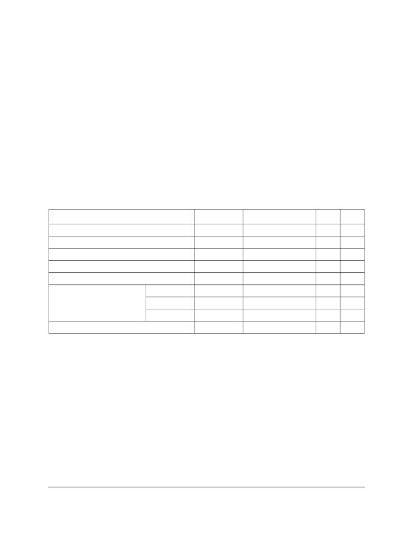
Table 1. Absolute Maximum Ratings
1
Characteristic
Symbol
Maximum Value
Unit
Notes
Core supply voltage
V
DD
–0.3 to 2.5
V
4
PLL supply voltage
AV
DD
–0.3 to 2.5
V
4
L2 DLL supply voltage
L2AV
DD
–0.3 to 2.5
V
4
Processor bus supply voltage
OV
DD
–0.3 to 3.6
V
3
L2 bus supply voltage
L2OV
DD
–0.3 to 3.6
V
3
Input voltage
Processor bus
V
in
–0.3 to OV
DD
+ 0.3 V
V
2, 5
L2 bus
V
in
–0.3 to L2OV
DD
+ 0.3 V
V
2, 5
JTAG signals
V
in
–0.3 to 3.6
V
Storage temperature range
T
stg
–55 to 150
°C
Notes:
1. Functional and tested operating conditions are given in Table 3. Absolute maximum ratings are stress ratings
only, and functional operation at the maximums is not guaranteed. Stresses beyond those listed may affect device
reliability or cause permanent damage to the device.
2.
Caution:
Vin must not exceed OV
DD
or L2OV
DD
by more than 0.3 V at any time including during power-on reset.
3.
Caution:
L2OV
DD
/OV
DD
must not exceed V
DD
/AV
DD
/L2AV
DD
by more than 1.6 V during normal operation; this
limit may be exceeded for a maximum of 20 ms during power-on reset and power-down sequences.
4.
Caution:
V
DD
/AV
DD
/L2AV
DD
must not exceed L2OV
DD
/OV
DD
by more than 0.4 V during normal operation; this
limit may be exceeded for a maximum of 20 ms during power-on reset and power-down sequences.
5. V
in
may overshoot/undershoot to a voltage and for a maximum duration as shown in Figure 2.
相關(guān)PDF資料 |
PDF描述 |
|---|---|
| XPC750EC | XPC750P/D XPC750P RISC Microprocessor Hardware Specifications |
| XPC801ZP25 | Microprocessor |
| XPC801ZP40 | Microprocessor |
| XPC821ZP40 | Microprocessor |
| XPC823ZP25 | Microprocessor |
相關(guān)代理商/技術(shù)參數(shù) |
參數(shù)描述 |
|---|---|
| XPC801ZP25 | 制造商:未知廠家 制造商全稱:未知廠家 功能描述:Microprocessor |
| XPC801ZP40 | 制造商:未知廠家 制造商全稱:未知廠家 功能描述:Microprocessor |
| XPC821ZP40 | 制造商:未知廠家 制造商全稱:未知廠家 功能描述:Microprocessor |
| XPC823CVR66B2T | 功能描述:IC MPU POWERQUICC 66MHZ 256-PBGA RoHS:是 類別:集成電路 (IC) >> 嵌入式 - 微處理器 系列:MPC8xx 標(biāo)準(zhǔn)包裝:2 系列:MPC8xx 處理器類型:32-位 MPC8xx PowerQUICC 特點:- 速度:133MHz 電壓:3.3V 安裝類型:表面貼裝 封裝/外殼:357-BBGA 供應(yīng)商設(shè)備封裝:357-PBGA(25x25) 包裝:托盤 |
| XPC823CZC66A | 制造商:Freescale Semiconductor 功能描述: |
發(fā)布緊急采購,3分鐘左右您將得到回復(fù)。