- 您現(xiàn)在的位置:買(mǎi)賣(mài)IC網(wǎng) > PDF目錄36338 > 935262469557 (NXP SEMICONDUCTORS) SPECIALTY CONSUMER CIRCUIT, PQFP240 PDF資料下載
參數(shù)資料
| 型號(hào): | 935262469557 |
| 廠(chǎng)商: | NXP SEMICONDUCTORS |
| 元件分類(lèi): | 消費(fèi)家電 |
| 英文描述: | SPECIALTY CONSUMER CIRCUIT, PQFP240 |
| 封裝: | 32 X 32 MM, 3.40 MM HEIGHT, MSQFP-240 |
| 文件頁(yè)數(shù): | 67/518頁(yè) |
| 文件大?。?/td> | 7111K |
| 代理商: | 935262469557 |
第1頁(yè)第2頁(yè)第3頁(yè)第4頁(yè)第5頁(yè)第6頁(yè)第7頁(yè)第8頁(yè)第9頁(yè)第10頁(yè)第11頁(yè)第12頁(yè)第13頁(yè)第14頁(yè)第15頁(yè)第16頁(yè)第17頁(yè)第18頁(yè)第19頁(yè)第20頁(yè)第21頁(yè)第22頁(yè)第23頁(yè)第24頁(yè)第25頁(yè)第26頁(yè)第27頁(yè)第28頁(yè)第29頁(yè)第30頁(yè)第31頁(yè)第32頁(yè)第33頁(yè)第34頁(yè)第35頁(yè)第36頁(yè)第37頁(yè)第38頁(yè)第39頁(yè)第40頁(yè)第41頁(yè)第42頁(yè)第43頁(yè)第44頁(yè)第45頁(yè)第46頁(yè)第47頁(yè)第48頁(yè)第49頁(yè)第50頁(yè)第51頁(yè)第52頁(yè)第53頁(yè)第54頁(yè)第55頁(yè)第56頁(yè)第57頁(yè)第58頁(yè)第59頁(yè)第60頁(yè)第61頁(yè)第62頁(yè)第63頁(yè)第64頁(yè)第65頁(yè)第66頁(yè)當(dāng)前第67頁(yè)第68頁(yè)第69頁(yè)第70頁(yè)第71頁(yè)第72頁(yè)第73頁(yè)第74頁(yè)第75頁(yè)第76頁(yè)第77頁(yè)第78頁(yè)第79頁(yè)第80頁(yè)第81頁(yè)第82頁(yè)第83頁(yè)第84頁(yè)第85頁(yè)第86頁(yè)第87頁(yè)第88頁(yè)第89頁(yè)第90頁(yè)第91頁(yè)第92頁(yè)第93頁(yè)第94頁(yè)第95頁(yè)第96頁(yè)第97頁(yè)第98頁(yè)第99頁(yè)第100頁(yè)第101頁(yè)第102頁(yè)第103頁(yè)第104頁(yè)第105頁(yè)第106頁(yè)第107頁(yè)第108頁(yè)第109頁(yè)第110頁(yè)第111頁(yè)第112頁(yè)第113頁(yè)第114頁(yè)第115頁(yè)第116頁(yè)第117頁(yè)第118頁(yè)第119頁(yè)第120頁(yè)第121頁(yè)第122頁(yè)第123頁(yè)第124頁(yè)第125頁(yè)第126頁(yè)第127頁(yè)第128頁(yè)第129頁(yè)第130頁(yè)第131頁(yè)第132頁(yè)第133頁(yè)第134頁(yè)第135頁(yè)第136頁(yè)第137頁(yè)第138頁(yè)第139頁(yè)第140頁(yè)第141頁(yè)第142頁(yè)第143頁(yè)第144頁(yè)第145頁(yè)第146頁(yè)第147頁(yè)第148頁(yè)第149頁(yè)第150頁(yè)第151頁(yè)第152頁(yè)第153頁(yè)第154頁(yè)第155頁(yè)第156頁(yè)第157頁(yè)第158頁(yè)第159頁(yè)第160頁(yè)第161頁(yè)第162頁(yè)第163頁(yè)第164頁(yè)第165頁(yè)第166頁(yè)第167頁(yè)第168頁(yè)第169頁(yè)第170頁(yè)第171頁(yè)第172頁(yè)第173頁(yè)第174頁(yè)第175頁(yè)第176頁(yè)第177頁(yè)第178頁(yè)第179頁(yè)第180頁(yè)第181頁(yè)第182頁(yè)第183頁(yè)第184頁(yè)第185頁(yè)第186頁(yè)第187頁(yè)第188頁(yè)第189頁(yè)第190頁(yè)第191頁(yè)第192頁(yè)第193頁(yè)第194頁(yè)第195頁(yè)第196頁(yè)第197頁(yè)第198頁(yè)第199頁(yè)第200頁(yè)第201頁(yè)第202頁(yè)第203頁(yè)第204頁(yè)第205頁(yè)第206頁(yè)第207頁(yè)第208頁(yè)第209頁(yè)第210頁(yè)第211頁(yè)第212頁(yè)第213頁(yè)第214頁(yè)第215頁(yè)第216頁(yè)第217頁(yè)第218頁(yè)第219頁(yè)第220頁(yè)第221頁(yè)第222頁(yè)第223頁(yè)第224頁(yè)第225頁(yè)第226頁(yè)第227頁(yè)第228頁(yè)第229頁(yè)第230頁(yè)第231頁(yè)第232頁(yè)第233頁(yè)第234頁(yè)第235頁(yè)第236頁(yè)第237頁(yè)第238頁(yè)第239頁(yè)第240頁(yè)第241頁(yè)第242頁(yè)第243頁(yè)第244頁(yè)第245頁(yè)第246頁(yè)第247頁(yè)第248頁(yè)第249頁(yè)第250頁(yè)第251頁(yè)第252頁(yè)第253頁(yè)第254頁(yè)第255頁(yè)第256頁(yè)第257頁(yè)第258頁(yè)第259頁(yè)第260頁(yè)第261頁(yè)第262頁(yè)第263頁(yè)第264頁(yè)第265頁(yè)第266頁(yè)第267頁(yè)第268頁(yè)第269頁(yè)第270頁(yè)第271頁(yè)第272頁(yè)第273頁(yè)第274頁(yè)第275頁(yè)第276頁(yè)第277頁(yè)第278頁(yè)第279頁(yè)第280頁(yè)第281頁(yè)第282頁(yè)第283頁(yè)第284頁(yè)第285頁(yè)第286頁(yè)第287頁(yè)第288頁(yè)第289頁(yè)第290頁(yè)第291頁(yè)第292頁(yè)第293頁(yè)第294頁(yè)第295頁(yè)第296頁(yè)第297頁(yè)第298頁(yè)第299頁(yè)第300頁(yè)第301頁(yè)第302頁(yè)第303頁(yè)第304頁(yè)第305頁(yè)第306頁(yè)第307頁(yè)第308頁(yè)第309頁(yè)第310頁(yè)第311頁(yè)第312頁(yè)第313頁(yè)第314頁(yè)第315頁(yè)第316頁(yè)第317頁(yè)第318頁(yè)第319頁(yè)第320頁(yè)第321頁(yè)第322頁(yè)第323頁(yè)第324頁(yè)第325頁(yè)第326頁(yè)第327頁(yè)第328頁(yè)第329頁(yè)第330頁(yè)第331頁(yè)第332頁(yè)第333頁(yè)第334頁(yè)第335頁(yè)第336頁(yè)第337頁(yè)第338頁(yè)第339頁(yè)第340頁(yè)第341頁(yè)第342頁(yè)第343頁(yè)第344頁(yè)第345頁(yè)第346頁(yè)第347頁(yè)第348頁(yè)第349頁(yè)第350頁(yè)第351頁(yè)第352頁(yè)第353頁(yè)第354頁(yè)第355頁(yè)第356頁(yè)第357頁(yè)第358頁(yè)第359頁(yè)第360頁(yè)第361頁(yè)第362頁(yè)第363頁(yè)第364頁(yè)第365頁(yè)第366頁(yè)第367頁(yè)第368頁(yè)第369頁(yè)第370頁(yè)第371頁(yè)第372頁(yè)第373頁(yè)第374頁(yè)第375頁(yè)第376頁(yè)第377頁(yè)第378頁(yè)第379頁(yè)第380頁(yè)第381頁(yè)第382頁(yè)第383頁(yè)第384頁(yè)第385頁(yè)第386頁(yè)第387頁(yè)第388頁(yè)第389頁(yè)第390頁(yè)第391頁(yè)第392頁(yè)第393頁(yè)第394頁(yè)第395頁(yè)第396頁(yè)第397頁(yè)第398頁(yè)第399頁(yè)第400頁(yè)第401頁(yè)第402頁(yè)第403頁(yè)第404頁(yè)第405頁(yè)第406頁(yè)第407頁(yè)第408頁(yè)第409頁(yè)第410頁(yè)第411頁(yè)第412頁(yè)第413頁(yè)第414頁(yè)第415頁(yè)第416頁(yè)第417頁(yè)第418頁(yè)第419頁(yè)第420頁(yè)第421頁(yè)第422頁(yè)第423頁(yè)第424頁(yè)第425頁(yè)第426頁(yè)第427頁(yè)第428頁(yè)第429頁(yè)第430頁(yè)第431頁(yè)第432頁(yè)第433頁(yè)第434頁(yè)第435頁(yè)第436頁(yè)第437頁(yè)第438頁(yè)第439頁(yè)第440頁(yè)第441頁(yè)第442頁(yè)第443頁(yè)第444頁(yè)第445頁(yè)第446頁(yè)第447頁(yè)第448頁(yè)第449頁(yè)第450頁(yè)第451頁(yè)第452頁(yè)第453頁(yè)第454頁(yè)第455頁(yè)第456頁(yè)第457頁(yè)第458頁(yè)第459頁(yè)第460頁(yè)第461頁(yè)第462頁(yè)第463頁(yè)第464頁(yè)第465頁(yè)第466頁(yè)第467頁(yè)第468頁(yè)第469頁(yè)第470頁(yè)第471頁(yè)第472頁(yè)第473頁(yè)第474頁(yè)第475頁(yè)第476頁(yè)第477頁(yè)第478頁(yè)第479頁(yè)第480頁(yè)第481頁(yè)第482頁(yè)第483頁(yè)第484頁(yè)第485頁(yè)第486頁(yè)第487頁(yè)第488頁(yè)第489頁(yè)第490頁(yè)第491頁(yè)第492頁(yè)第493頁(yè)第494頁(yè)第495頁(yè)第496頁(yè)第497頁(yè)第498頁(yè)第499頁(yè)第500頁(yè)第501頁(yè)第502頁(yè)第503頁(yè)第504頁(yè)第505頁(yè)第506頁(yè)第507頁(yè)第508頁(yè)第509頁(yè)第510頁(yè)第511頁(yè)第512頁(yè)第513頁(yè)第514頁(yè)第515頁(yè)第516頁(yè)第517頁(yè)第518頁(yè)
Philips Semiconductors
PCI Interface
File: pci.fm5, modified 7/23/99
PRELIMINARY INFORMATION
10-15
The DMA destination address is cache line size
aligned.
The T bit is set
TM1100 generates “memory read multiple” PCI transac-
tions for DMA reads, unless the RMD (Read Multiple Dis-
able) bit is set in BIU_CTL, in which case the less effi-
cient “memory read” transactions are used.
During a PCI
→ SDRAM block transfer, the PCI interface
drives the PCI bus with the address from SRC_ADR. The
returned data is buffered in r_buffer. The PCI interface
then drives the address from DEST_ADR and the data
from r_buffer to the SDRAM controller. SRC_ADR and
DEST_ADR are incremented, the TL field in DMA_CTL
is decremented, and this sequence repeats until TL
reaches zero.
At the end of the PCI
→ SDRAM block transfer, the PCI
interface will generate a DSPCPU interrupt if the appro-
priate IntE bit is set in BIU_CTL. Alternatively, DSPCPU
software can poll the appropriate “done” status bin in
BIU_STATUS.
During an SDRAM
→ PCI block transfer, the PCI inter-
face drives the address from SRC_ADR to the SDRAM
controller. The returned data is buffered in w_buffer. The
PCI interface then drives the address from DEST_ADR
and the data from w_buffer to the PCI bus. SRC_ADR
and DEST_ADR are incremented, the TL field in
DMA_CTL is decremented, and this sequence repeats
until TL reaches zero.
At the end of the SDRAM
→ PCI block transfer, the PCI
interface can generate a DSPCPU interrupt if the appro-
priate IntE bit is set in BIU_CTL. Alternatively, DSPCPU
software can poll the appropriate “done” status bit in
BIU_STATUS.
10.7.17 INT_CTL Register
The INT_CTL register contains three fields for setting,
enabling, and sensing the four PCI interrupt lines.
Table 10-19 shows the interpretation of the fields in
INT_CTL.
INT (Interrupt bits). The INT field (bits 0..3 of INT_CTL)
can force a PCI interrupt to be signalled.
IE (Interrupt Enable). The IE field (bits 4..7 of INT_CTL)
enables TM1100 to drive PCI interrupt lines.
IS (Interrupt State). The IS field (bits 8..11 of INT_CTL)
senses the state of the PCI interrupt lines.
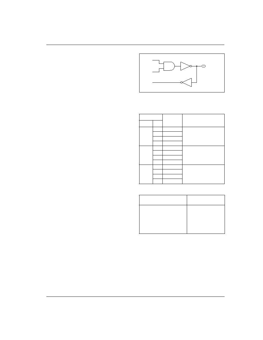
Figure 10-9 shows a conceptual realization of the logic
used to implement the control of each intx# pin.
10.8
PCI BUS PROTOCOL OVERVIEW
TM1100’s PCI interface can generate and respond to
several types of PCI bus commands. Table 10-20 lists
the 12 possible commands and whether or not TM1100
Table 10-21 lists the 12 possible commands and wheth-
er or not TM1100 can respond to them.
The basic transfer mechanism on the PCI bus is a burst,
which consists of an address phase followed by one or
more data phases. In TM1100, the DSPCPU and Image
Coprocessor (ICP) are the only two units that can cause
TM1100 to become a PCI-bus initiator; i.e., only the
DSPCPU and ICP can access external resources.
Table 10-19. INT_CTL Bits
INT_CTL
PCI Signal
Programming
Field
Bit
INT
0
inta#
0
Deassert intx#
1
Assert intx# (if enabled);
i.e., pull intx# pin to a low
logic level
1
intb#
2
intc#
3
intd#
IE
4
inta#
0
Disable open-collector
output to intx#
1
Enable open-collector
output to intx#
5
intb#
6
intc#
7
intd#
IS
8
inta#
Reads state of intx# pin:
0
No interrupt asserted
(intx# is high)
1
Interrupt is asserted
(intx# is low)
9
intb#
10
intc#
11
intd#
Table 10-20. TM1100 PCI Commands as Initiator
TM1100 Generates
TM1100 Cannot
Generate
Conguration read
Conguration write
Memory read
Memory read multiple
Memory write
Memory write and invalidate
I/O read
I/O write
Interrupt acknowledge
Special cycle
Dual address
Memory read line
INTx
oc
PCI intx#
IEx
ISx
Figure 10-9. Conceptual realization of intx# pin con-
trol logic.
相關(guān)PDF資料 |
PDF描述 |
|---|---|
| 935263151557 | SPECIALTY CONSUMER CIRCUIT, PQFP240 |
| 935263331557 | SPECIALTY CONSUMER CIRCUIT, PQFP240 |
| 935263133112 | 26 W, 1 CHANNEL, AUDIO AMPLIFIER, PZIP17 |
| 935263384118 | SPECIALTY ANALOG CIRCUIT, PDSO16 |
| 935263384112 | SPECIALTY ANALOG CIRCUIT, PDSO16 |
相關(guān)代理商/技術(shù)參數(shù) |
參數(shù)描述 |
|---|---|
| 935264217557 | 制造商:NXP Semiconductors 功能描述:SUB ONLY IC |
| 935267356112 | 制造商:NXP Semiconductors 功能描述:IC TEA1507PN |
| 935268081112 | 制造商:NXP Semiconductors 功能描述:SUB ONLY IC |
| 935268721125 | 制造商:NXP Semiconductors 功能描述:Buffer/Line Driver 1-CH Non-Inverting 3-ST CMOS 5-Pin TSSOP T/R |
| 935269304128 | 制造商:ST-Ericsson 功能描述:IC AUDIO CODEC W/TCH SCRN 48LQFP |
發(fā)布緊急采購(gòu),3分鐘左右您將得到回復(fù)。