- 您現(xiàn)在的位置:買賣IC網(wǎng) > PDF目錄36338 > 935262469557 (NXP SEMICONDUCTORS) SPECIALTY CONSUMER CIRCUIT, PQFP240 PDF資料下載
參數(shù)資料
| 型號: | 935262469557 |
| 廠商: | NXP SEMICONDUCTORS |
| 元件分類: | 消費家電 |
| 英文描述: | SPECIALTY CONSUMER CIRCUIT, PQFP240 |
| 封裝: | 32 X 32 MM, 3.40 MM HEIGHT, MSQFP-240 |
| 文件頁數(shù): | 78/518頁 |
| 文件大小: | 7111K |
| 代理商: | 935262469557 |
第1頁第2頁第3頁第4頁第5頁第6頁第7頁第8頁第9頁第10頁第11頁第12頁第13頁第14頁第15頁第16頁第17頁第18頁第19頁第20頁第21頁第22頁第23頁第24頁第25頁第26頁第27頁第28頁第29頁第30頁第31頁第32頁第33頁第34頁第35頁第36頁第37頁第38頁第39頁第40頁第41頁第42頁第43頁第44頁第45頁第46頁第47頁第48頁第49頁第50頁第51頁第52頁第53頁第54頁第55頁第56頁第57頁第58頁第59頁第60頁第61頁第62頁第63頁第64頁第65頁第66頁第67頁第68頁第69頁第70頁第71頁第72頁第73頁第74頁第75頁第76頁第77頁當(dāng)前第78頁第79頁第80頁第81頁第82頁第83頁第84頁第85頁第86頁第87頁第88頁第89頁第90頁第91頁第92頁第93頁第94頁第95頁第96頁第97頁第98頁第99頁第100頁第101頁第102頁第103頁第104頁第105頁第106頁第107頁第108頁第109頁第110頁第111頁第112頁第113頁第114頁第115頁第116頁第117頁第118頁第119頁第120頁第121頁第122頁第123頁第124頁第125頁第126頁第127頁第128頁第129頁第130頁第131頁第132頁第133頁第134頁第135頁第136頁第137頁第138頁第139頁第140頁第141頁第142頁第143頁第144頁第145頁第146頁第147頁第148頁第149頁第150頁第151頁第152頁第153頁第154頁第155頁第156頁第157頁第158頁第159頁第160頁第161頁第162頁第163頁第164頁第165頁第166頁第167頁第168頁第169頁第170頁第171頁第172頁第173頁第174頁第175頁第176頁第177頁第178頁第179頁第180頁第181頁第182頁第183頁第184頁第185頁第186頁第187頁第188頁第189頁第190頁第191頁第192頁第193頁第194頁第195頁第196頁第197頁第198頁第199頁第200頁第201頁第202頁第203頁第204頁第205頁第206頁第207頁第208頁第209頁第210頁第211頁第212頁第213頁第214頁第215頁第216頁第217頁第218頁第219頁第220頁第221頁第222頁第223頁第224頁第225頁第226頁第227頁第228頁第229頁第230頁第231頁第232頁第233頁第234頁第235頁第236頁第237頁第238頁第239頁第240頁第241頁第242頁第243頁第244頁第245頁第246頁第247頁第248頁第249頁第250頁第251頁第252頁第253頁第254頁第255頁第256頁第257頁第258頁第259頁第260頁第261頁第262頁第263頁第264頁第265頁第266頁第267頁第268頁第269頁第270頁第271頁第272頁第273頁第274頁第275頁第276頁第277頁第278頁第279頁第280頁第281頁第282頁第283頁第284頁第285頁第286頁第287頁第288頁第289頁第290頁第291頁第292頁第293頁第294頁第295頁第296頁第297頁第298頁第299頁第300頁第301頁第302頁第303頁第304頁第305頁第306頁第307頁第308頁第309頁第310頁第311頁第312頁第313頁第314頁第315頁第316頁第317頁第318頁第319頁第320頁第321頁第322頁第323頁第324頁第325頁第326頁第327頁第328頁第329頁第330頁第331頁第332頁第333頁第334頁第335頁第336頁第337頁第338頁第339頁第340頁第341頁第342頁第343頁第344頁第345頁第346頁第347頁第348頁第349頁第350頁第351頁第352頁第353頁第354頁第355頁第356頁第357頁第358頁第359頁第360頁第361頁第362頁第363頁第364頁第365頁第366頁第367頁第368頁第369頁第370頁第371頁第372頁第373頁第374頁第375頁第376頁第377頁第378頁第379頁第380頁第381頁第382頁第383頁第384頁第385頁第386頁第387頁第388頁第389頁第390頁第391頁第392頁第393頁第394頁第395頁第396頁第397頁第398頁第399頁第400頁第401頁第402頁第403頁第404頁第405頁第406頁第407頁第408頁第409頁第410頁第411頁第412頁第413頁第414頁第415頁第416頁第417頁第418頁第419頁第420頁第421頁第422頁第423頁第424頁第425頁第426頁第427頁第428頁第429頁第430頁第431頁第432頁第433頁第434頁第435頁第436頁第437頁第438頁第439頁第440頁第441頁第442頁第443頁第444頁第445頁第446頁第447頁第448頁第449頁第450頁第451頁第452頁第453頁第454頁第455頁第456頁第457頁第458頁第459頁第460頁第461頁第462頁第463頁第464頁第465頁第466頁第467頁第468頁第469頁第470頁第471頁第472頁第473頁第474頁第475頁第476頁第477頁第478頁第479頁第480頁第481頁第482頁第483頁第484頁第485頁第486頁第487頁第488頁第489頁第490頁第491頁第492頁第493頁第494頁第495頁第496頁第497頁第498頁第499頁第500頁第501頁第502頁第503頁第504頁第505頁第506頁第507頁第508頁第509頁第510頁第511頁第512頁第513頁第514頁第515頁第516頁第517頁第518頁
Philips Semiconductors
SDRAM Memory System
File: memsys.fm5, modified 7/24/99
PRELIMINARY INFORMATION
11-7
clock and matchout signals have source-series termina-
tion. The matchout/matchin trace has a lumped load es-
timating two SDRAM clock input and data loads.
It is recommended to abandon the transmission line
MATCHOUT-MATCHIN for speed higher than 100 MHz.
Instead, tie MATCHOUT to MATCHIN through a RC de-
lay circuit with minimal wire-length. I.e. MATCHOUT
feeds a resistor R to MATCHIN. MATCHIN has a cap. C
to ground. Suitable values for R and C can be optimized
to get best performance out of a given board. Initially use
R = 0 Ohm, C = 0 pF, i.e. no C and shorted R. This will
work fine, and the fact that a R and C site are on the
board allows future fine-tuning. Figure 11-10 shows an
example for a 16 MB memory system.
11.14 CIRCUIT BOARD DESIGN
TM1100 and its memory array form a high-speed digital
system. Even though only a small number of chips is in-
volved, this digital system operates at frequencies high
enough to make the analog characteristics of the con-
nections between the chips significant. Consequently,
the system designer must take care to ensure reliable
operation.
11.14.1 General Guidelines
In general, TM1100 and its memory chips should be
as close together as possible to minimize parasitic
capacitance. Close proximity is especially important
for a 100-MHz or higher memory system.
SIgnal traces between TM1100 and the memory
chips should be matched in length as closely as pos-
sible to minimize signal skew.
The clock-signal trace(s) should be as short as pos-
sible.
Address and control-signal traces should also be
short, but their length is less critical than the clock’s.
Data-signal traces should also be short, but their
length is less critical than the clock’s, especially if
only one or two ranks are connected.
The length of the trace between matchout and
matchin should be as close as possible to the sum of
the lengths of the longest clock and data traces.
11.14.2 Specific Guidelines
The maximum length for a signal trace is 10 cm.
The maximum capacitive load is 30 pF per trace,
including loads.
The signal traces on the TM1100 circuit board must
be designed as 50-Ohm transmission lines.
At 100 MHz or higher, the memory chips should also
be soldered to the circuit board.
At most two SDRAM devices may be connected to
each MM_CLK signal at 133 MHz.
11.14.3 Termination
No termination is required for address, data, and control
signals. Address and control signals are driven only by
TM1100; the output impedance of the drivers is suffi-
ciently matched to prevent excessive ringing. TM1100
design assumes that the output drivers of SDRAM chips,
when driving data lines, are also sufficiently impedance
matched.
Series termination of the clock and matchout outputs
with a 22-Ohm resister is advised when operating the
memory system at 100-MHz or higher (see Section
11.15 TIMING BUDGET
The glueless interface of the TM1100 main-memory in-
terface makes the memory system simple and straight-
forward from one point of view, but to ensure reliable op-
eration at high clock rates, system designers must follow
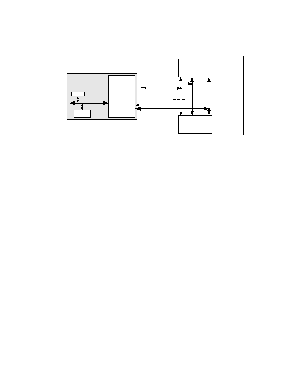
Figure 11-4. Conceptual board layout. The match trace loop should be as close to the sum of the lengths of
the clock and data traces as possible.
Address
&
Control
CLK
DQ[31:0]
GND
22
22
Address
&
Control
CLK
DQ[31:0]
14 pF
SDRAM
Device
SDRAM
Device
TM1100
Memory
Interface
Address,
Clock Enables,
RAS#, CAS#, WE#
Clock
MatchOut
MatchIn
Data[31:0]
Data
Highway
TM1100
On-Chip
Peripherals
DSPCPU
相關(guān)PDF資料 |
PDF描述 |
|---|---|
| 935263151557 | SPECIALTY CONSUMER CIRCUIT, PQFP240 |
| 935263331557 | SPECIALTY CONSUMER CIRCUIT, PQFP240 |
| 935263133112 | 26 W, 1 CHANNEL, AUDIO AMPLIFIER, PZIP17 |
| 935263384118 | SPECIALTY ANALOG CIRCUIT, PDSO16 |
| 935263384112 | SPECIALTY ANALOG CIRCUIT, PDSO16 |
相關(guān)代理商/技術(shù)參數(shù) |
參數(shù)描述 |
|---|---|
| 935264217557 | 制造商:NXP Semiconductors 功能描述:SUB ONLY IC |
| 935267356112 | 制造商:NXP Semiconductors 功能描述:IC TEA1507PN |
| 935268081112 | 制造商:NXP Semiconductors 功能描述:SUB ONLY IC |
| 935268721125 | 制造商:NXP Semiconductors 功能描述:Buffer/Line Driver 1-CH Non-Inverting 3-ST CMOS 5-Pin TSSOP T/R |
| 935269304128 | 制造商:ST-Ericsson 功能描述:IC AUDIO CODEC W/TCH SCRN 48LQFP |
發(fā)布緊急采購,3分鐘左右您將得到回復(fù)。