- 您現(xiàn)在的位置:買賣IC網(wǎng) > PDF目錄45188 > MB90P663AP-SH 16-BIT, OTPROM, 16 MHz, MICROCONTROLLER, PDIP64 PDF資料下載
參數(shù)資料
| 型號: | MB90P663AP-SH |
| 元件分類: | 微控制器/微處理器 |
| 英文描述: | 16-BIT, OTPROM, 16 MHz, MICROCONTROLLER, PDIP64 |
| 封裝: | PLASTIC, SHRINK, DIP-64 |
| 文件頁數(shù): | 257/284頁 |
| 文件大小: | 2703K |
| 代理商: | MB90P663AP-SH |
第1頁第2頁第3頁第4頁第5頁第6頁第7頁第8頁第9頁第10頁第11頁第12頁第13頁第14頁第15頁第16頁第17頁第18頁第19頁第20頁第21頁第22頁第23頁第24頁第25頁第26頁第27頁第28頁第29頁第30頁第31頁第32頁第33頁第34頁第35頁第36頁第37頁第38頁第39頁第40頁第41頁第42頁第43頁第44頁第45頁第46頁第47頁第48頁第49頁第50頁第51頁第52頁第53頁第54頁第55頁第56頁第57頁第58頁第59頁第60頁第61頁第62頁第63頁第64頁第65頁第66頁第67頁第68頁第69頁第70頁第71頁第72頁第73頁第74頁第75頁第76頁第77頁第78頁第79頁第80頁第81頁第82頁第83頁第84頁第85頁第86頁第87頁第88頁第89頁第90頁第91頁第92頁第93頁第94頁第95頁第96頁第97頁第98頁第99頁第100頁第101頁第102頁第103頁第104頁第105頁第106頁第107頁第108頁第109頁第110頁第111頁第112頁第113頁第114頁第115頁第116頁第117頁第118頁第119頁第120頁第121頁第122頁第123頁第124頁第125頁第126頁第127頁第128頁第129頁第130頁第131頁第132頁第133頁第134頁第135頁第136頁第137頁第138頁第139頁第140頁第141頁第142頁第143頁第144頁第145頁第146頁第147頁第148頁第149頁第150頁第151頁第152頁第153頁第154頁第155頁第156頁第157頁第158頁第159頁第160頁第161頁第162頁第163頁第164頁第165頁第166頁第167頁第168頁第169頁第170頁第171頁第172頁第173頁第174頁第175頁第176頁第177頁第178頁第179頁第180頁第181頁第182頁第183頁第184頁第185頁第186頁第187頁第188頁第189頁第190頁第191頁第192頁第193頁第194頁第195頁第196頁第197頁第198頁第199頁第200頁第201頁第202頁第203頁第204頁第205頁第206頁第207頁第208頁第209頁第210頁第211頁第212頁第213頁第214頁第215頁第216頁第217頁第218頁第219頁第220頁第221頁第222頁第223頁第224頁第225頁第226頁第227頁第228頁第229頁第230頁第231頁第232頁第233頁第234頁第235頁第236頁第237頁第238頁第239頁第240頁第241頁第242頁第243頁第244頁第245頁第246頁第247頁第248頁第249頁第250頁第251頁第252頁第253頁第254頁第255頁第256頁當前第257頁第258頁第259頁第260頁第261頁第262頁第263頁第264頁第265頁第266頁第267頁第268頁第269頁第270頁第271頁第272頁第273頁第274頁第275頁第276頁第277頁第278頁第279頁第280頁第281頁第282頁第283頁第284頁
2.3 Parallel Ports
69
(2) DDR 0, 1, 2, 3, 4, 6 (Port direction registers)
s Register Allocation
[CAUTION]
Port 3 bits 15 to 12 have no register bit.
Port 4 bit 7 has no register bit.
Port 5 has no DDR.
Port 6 bit 7 has no register bit.
s Register Description
When the corresponding signal pins are functioning as ports, the function of each pin is controlled as
follows.
0: Input mode
1: Output mode
Values are initialized to ‘0’ at a reset.
[CAUTION]
Port 6 should be placed in output mode when it is used as a multi-function timer output
pin.
(3) ADER (Analog input enable register)
s Register Description
Port 5 signal pins are controlled as follows.
0: Port input mode
1: Analog input mode
The reset value is ‘1.’
[CAUTION]
Be sure to select analog input mode whenever this port is used for analog input. This is
because input of intermediate-level signals in port input mode will produce leak current.
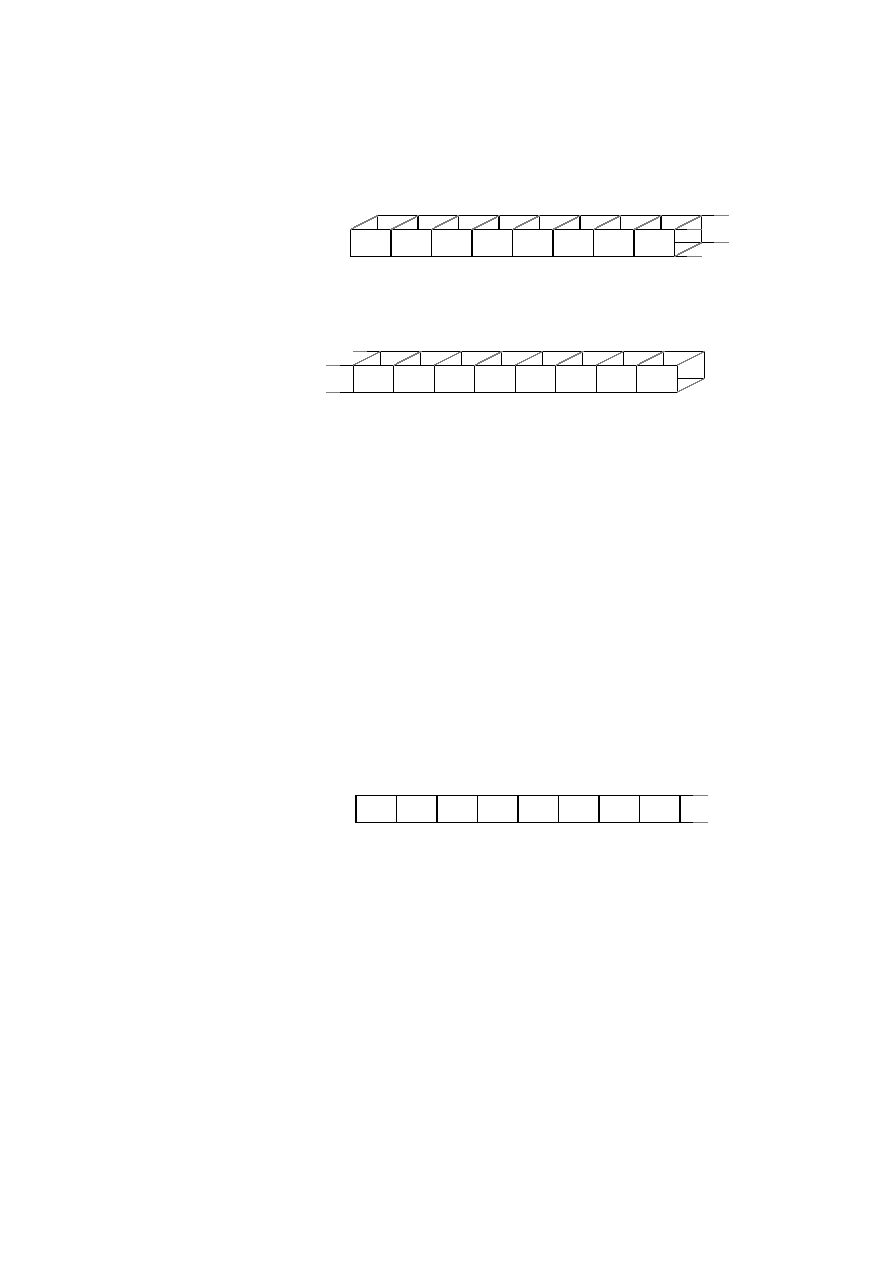
DDx7 DDx6 DDx5 DDx4 DDx3 DDx2 DDx1 DDx0
Port direction register
Address : DDR1 000011H
Bit no.
Read/write
(R/W) (R/W) (R/W) (R/W) (R/W) (R/W) (R/W) (R/W)
Initial value
(0)
DDR3 000013H
15
14
13
12
11
10
9
8
DDx7 DDx6 DDx5 DDx4 DDx3 DDx2 DDx1 DDx0
Bit no.
Read/write
(R/W) (R/W) (R/W) (R/W) (R/W) (R/W) (R/W) (R/W)
Initial value
(0)
Port direction register
Address : DDR0 000010H
DDR2 000012H
7
6
5
4
3
2
1
0
DDRx
DDR4 000014H
DDR6 000016H
DDRx
ADE7 ADE6 ADE5 ADE4 ADE3 ADE2 ADE1 ADE0
Bit no.
Read/write
(R/W) (R/W) (R/W) (R/W) (R/W) (R/W) (R/W) (R/W)
Initial value
(1)
Analog input enable register
Address : 000015H
15
14
13
12
11
10
9
8
ADER
相關(guān)PDF資料 |
PDF描述 |
|---|---|
| MB90673PF | 16-BIT, MROM, 16 MHz, MICROCONTROLLER, PQFP80 |
| MB90T673PF | 16-BIT, 16 MHz, MICROCONTROLLER, PQFP80 |
| MB90671PFV | 16-BIT, MROM, 16 MHz, MICROCONTROLLER, PQFP80 |
| MB90671PF | 16-BIT, MROM, 16 MHz, MICROCONTROLLER, PQFP80 |
| MB90P678PF | 16-BIT, OTPROM, 16 MHz, MICROCONTROLLER, PQFP100 |
相關(guān)代理商/技術(shù)參數(shù) |
參數(shù)描述 |
|---|---|
| MB90V340A-102CR | 制造商:FUJITSU 功能描述: |
| MB-910 | 制造商:Circuit Test 功能描述:BREADBOARD WIRING KIT - 350 PCS |
| MB9100100 | 制造商:COM/DUO 功能描述:FAN 4-6WKS |
| MB9100-100 | 制造商:COM/DUO 功能描述:FAN 4-6WKS |
| MB91101 | 制造商:Panasonic Industrial Company 功能描述:IC |
發(fā)布緊急采購,3分鐘左右您將得到回復。