- 您現在的位置:買賣IC網 > PDF目錄359234 > MT90520 (Zarlink Semiconductor Inc.) 8-Port Primary Rate Circuit Emulation AAL1 SAR PDF資料下載
參數資料
| 型號: | MT90520 |
| 廠商: | Zarlink Semiconductor Inc. |
| 英文描述: | 8-Port Primary Rate Circuit Emulation AAL1 SAR |
| 中文描述: | 8端口基本速率電路仿真AAL1特區(qū) |
| 文件頁數: | 148/180頁 |
| 文件大小: | 1736K |
| 代理商: | MT90520 |
第1頁第2頁第3頁第4頁第5頁第6頁第7頁第8頁第9頁第10頁第11頁第12頁第13頁第14頁第15頁第16頁第17頁第18頁第19頁第20頁第21頁第22頁第23頁第24頁第25頁第26頁第27頁第28頁第29頁第30頁第31頁第32頁第33頁第34頁第35頁第36頁第37頁第38頁第39頁第40頁第41頁第42頁第43頁第44頁第45頁第46頁第47頁第48頁第49頁第50頁第51頁第52頁第53頁第54頁第55頁第56頁第57頁第58頁第59頁第60頁第61頁第62頁第63頁第64頁第65頁第66頁第67頁第68頁第69頁第70頁第71頁第72頁第73頁第74頁第75頁第76頁第77頁第78頁第79頁第80頁第81頁第82頁第83頁第84頁第85頁第86頁第87頁第88頁第89頁第90頁第91頁第92頁第93頁第94頁第95頁第96頁第97頁第98頁第99頁第100頁第101頁第102頁第103頁第104頁第105頁第106頁第107頁第108頁第109頁第110頁第111頁第112頁第113頁第114頁第115頁第116頁第117頁第118頁第119頁第120頁第121頁第122頁第123頁第124頁第125頁第126頁第127頁第128頁第129頁第130頁第131頁第132頁第133頁第134頁第135頁第136頁第137頁第138頁第139頁第140頁第141頁第142頁第143頁第144頁第145頁第146頁第147頁當前第148頁第149頁第150頁第151頁第152頁第153頁第154頁第155頁第156頁第157頁第158頁第159頁第160頁第161頁第162頁第163頁第164頁第165頁第166頁第167頁第168頁第169頁第170頁第171頁第172頁第173頁第174頁第175頁第176頁第177頁第178頁第179頁第180頁
MT90520
Data Sheet
148
Zarlink Semiconductor Inc.
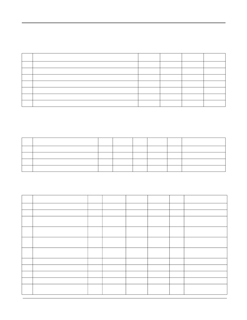
7.0 Electrical Specification
7.1 DC Characteristics
* Exceeding these figures may cause permanent damage. Functional operation under these conditions is not guaranteed.
Voltage measurements are with respect to ground (V
) unless otherwise stated. Long-term exposure to absolute maximum ratings may affect
device reliability, and exceeding the maximum ratings may cause permanent damage. The device should be operated under recommended
operating conditions.
Absolute Maximum Ratings
Parameter
Symbol
Min.
Max.
Units
1
Supply Voltage - 2.5 Volt Rail
V
DD2
V
SS
3.5
V
2
Supply Voltage - 3.3 Volt Rail
V
DD3
V
SS
4.5
V
3
Voltage on 3.3 V Input pins
V
I3
- 0.5
6
V
4
Voltage on 3.3 V Output pins
V
O3
- 0.5
4.6
V
5
Continuous current at digital inputs
I
I
±
10
mA
6
Continuous current at digital outputs
I
O
±
24
mA
7
Storage Temperature
T
S
- 40
+125
°
C
Recommended Operating Conditions
Characteristics
Sym.
Min.
Typ.
a
a. Typical figures are at 25
°
C and are for design aid only; not guaranteed and not subject to production testing.
Voltage measurements are with respect to ground (V
SS
) unless otherwise stated.
Max.
Units
Test Conditions
1
Operating Temperature
T
OP
- 40
25
+ 85
°
C
2
Supply
Voltage, 2.5 Volt Rail
V
DD2
2.37
2.5
2.63
V
3
Supply Voltage, 3.3 Volt Rail
V
DD3
3.13
3.3
3.46
V
4
Input Voltage, 3.3 V inputs
V
I3
- 0.5
5.5
V
DC Characteristics
Characteristics
Sym.
Min.
Typ.
a
Max.
Units
Test Conditions
b
1
Supply Current - 2.5 V supply
I
DD2
395
590
mA
66.0 MHz, UDT mode
2
Supply Current - 2.5 V supply
I
DD2
400
620
mA
66.0 MHz, SDT mode
3
Supply Current - 3.3 V supply
I
DD3
16
42
mA
66.0 MHz, UDT mode,
Notes 1, 2
4
Supply Current - 3.3 V supply
I
DD3
24
57
mA
66.0 MHz, SDT mode,
Notes 1, 3
5
Device Power Dissipation
(2.5 V and 3.3 V supplies)
P
DDU
1.0
1.7
W
66.0 MHz, UDT mode,
Notes 1, 2
6
Device Power Dissipation
(2.5 V and 3.3 V supplies)
P
DDS
1.1
1.8
W
66.0 MHz, SDT mode,
Notes 1, 3
7
Input High Voltage (3.3 V CMOS)
V
IH3
2.3
5.5
V
8
Input Low Voltage (3.3 V CMOS)
V
IL3
-0.5
1.0
V
9
Switching Threshold (3.3 V CMOS)
V
TC3
V
t+
V
t-
1.24
1.36
1.59
V
10
Schmitt Trigger Positive Threshold
1.57
1.72
V
11
Schmitt
Threshold
Trigger
Negative
0.825
1.18
V
相關PDF資料 |
PDF描述 |
|---|---|
| MT90520AG | 8-Port Primary Rate Circuit Emulation AAL1 SAR |
| MT9072 | Ultraframer DS3/E3/DS2/E2/DS1/E1/DS0 |
| MT9072AB | Ultraframer DS3/E3/DS2/E2/DS1/E1/DS0 |
| MT9072AV | Ultraframer DS3/E3/DS2/E2/DS1/E1/DS0 |
| MT90820 | Large Digital Switch |
相關代理商/技術參數 |
參數描述 |
|---|---|
| MT90520AG | 制造商:Microsemi Corporation 功能描述:ATM SAR 2.048MBPS 2.5V CBR 456BGA - Trays |
| MT90520AG2 | 制造商:Microsemi Corporation 功能描述:ATM SAR 2.048MBPS 2.5V CBR 456BGA - Trays 制造商:Zarlink Semiconductor Inc 功能描述:ATM SAR 2.048MBPS 2.5V CBR 456BGA - Trays |
| MT90528 | 制造商:ZARLINK 制造商全稱:Zarlink Semiconductor Inc 功能描述:28-Port Primary Rate Circuit Emulation AAL1 SAR |
| MT90528AG | 制造商:ZARLINK 制造商全稱:Zarlink Semiconductor Inc 功能描述:28-Port Primary Rate Circuit Emulation AAL1 SAR |
| MT90528AG2 | 制造商:ZARLINK 制造商全稱:Zarlink Semiconductor Inc 功能描述:28-Port Primary Rate Circuit Emulation AAL1 SAR |
發(fā)布緊急采購,3分鐘左右您將得到回復。