- 您現(xiàn)在的位置:買賣IC網(wǎng) > PDF目錄359234 > MT90520 (Zarlink Semiconductor Inc.) 8-Port Primary Rate Circuit Emulation AAL1 SAR PDF資料下載
參數(shù)資料
| 型號(hào): | MT90520 |
| 廠商: | Zarlink Semiconductor Inc. |
| 英文描述: | 8-Port Primary Rate Circuit Emulation AAL1 SAR |
| 中文描述: | 8端口基本速率電路仿真AAL1特區(qū) |
| 文件頁(yè)數(shù): | 68/180頁(yè) |
| 文件大?。?/td> | 1736K |
| 代理商: | MT90520 |
第1頁(yè)第2頁(yè)第3頁(yè)第4頁(yè)第5頁(yè)第6頁(yè)第7頁(yè)第8頁(yè)第9頁(yè)第10頁(yè)第11頁(yè)第12頁(yè)第13頁(yè)第14頁(yè)第15頁(yè)第16頁(yè)第17頁(yè)第18頁(yè)第19頁(yè)第20頁(yè)第21頁(yè)第22頁(yè)第23頁(yè)第24頁(yè)第25頁(yè)第26頁(yè)第27頁(yè)第28頁(yè)第29頁(yè)第30頁(yè)第31頁(yè)第32頁(yè)第33頁(yè)第34頁(yè)第35頁(yè)第36頁(yè)第37頁(yè)第38頁(yè)第39頁(yè)第40頁(yè)第41頁(yè)第42頁(yè)第43頁(yè)第44頁(yè)第45頁(yè)第46頁(yè)第47頁(yè)第48頁(yè)第49頁(yè)第50頁(yè)第51頁(yè)第52頁(yè)第53頁(yè)第54頁(yè)第55頁(yè)第56頁(yè)第57頁(yè)第58頁(yè)第59頁(yè)第60頁(yè)第61頁(yè)第62頁(yè)第63頁(yè)第64頁(yè)第65頁(yè)第66頁(yè)第67頁(yè)當(dāng)前第68頁(yè)第69頁(yè)第70頁(yè)第71頁(yè)第72頁(yè)第73頁(yè)第74頁(yè)第75頁(yè)第76頁(yè)第77頁(yè)第78頁(yè)第79頁(yè)第80頁(yè)第81頁(yè)第82頁(yè)第83頁(yè)第84頁(yè)第85頁(yè)第86頁(yè)第87頁(yè)第88頁(yè)第89頁(yè)第90頁(yè)第91頁(yè)第92頁(yè)第93頁(yè)第94頁(yè)第95頁(yè)第96頁(yè)第97頁(yè)第98頁(yè)第99頁(yè)第100頁(yè)第101頁(yè)第102頁(yè)第103頁(yè)第104頁(yè)第105頁(yè)第106頁(yè)第107頁(yè)第108頁(yè)第109頁(yè)第110頁(yè)第111頁(yè)第112頁(yè)第113頁(yè)第114頁(yè)第115頁(yè)第116頁(yè)第117頁(yè)第118頁(yè)第119頁(yè)第120頁(yè)第121頁(yè)第122頁(yè)第123頁(yè)第124頁(yè)第125頁(yè)第126頁(yè)第127頁(yè)第128頁(yè)第129頁(yè)第130頁(yè)第131頁(yè)第132頁(yè)第133頁(yè)第134頁(yè)第135頁(yè)第136頁(yè)第137頁(yè)第138頁(yè)第139頁(yè)第140頁(yè)第141頁(yè)第142頁(yè)第143頁(yè)第144頁(yè)第145頁(yè)第146頁(yè)第147頁(yè)第148頁(yè)第149頁(yè)第150頁(yè)第151頁(yè)第152頁(yè)第153頁(yè)第154頁(yè)第155頁(yè)第156頁(yè)第157頁(yè)第158頁(yè)第159頁(yè)第160頁(yè)第161頁(yè)第162頁(yè)第163頁(yè)第164頁(yè)第165頁(yè)第166頁(yè)第167頁(yè)第168頁(yè)第169頁(yè)第170頁(yè)第171頁(yè)第172頁(yè)第173頁(yè)第174頁(yè)第175頁(yè)第176頁(yè)第177頁(yè)第178頁(yè)第179頁(yè)第180頁(yè)
MT90520
Data Sheet
68
Zarlink Semiconductor Inc.
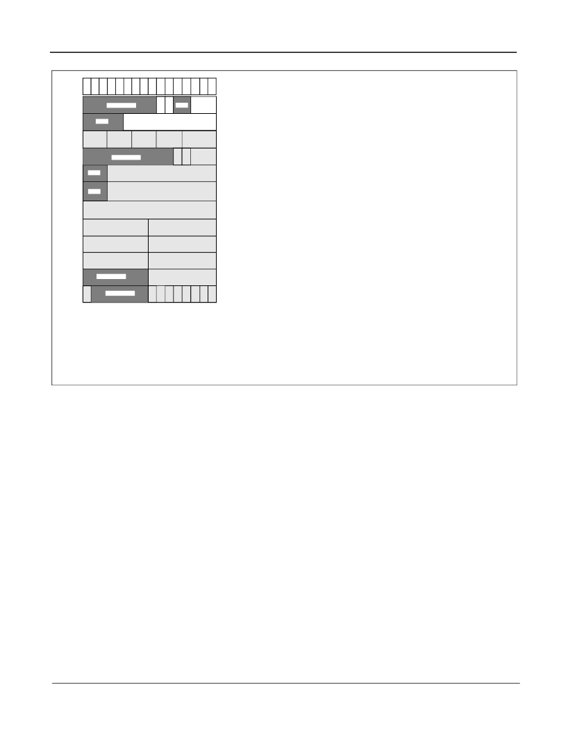
Figure 27 - Reassembly Control Structure - UDT Format
SDT Reassembly Control Structures
Within the SDT RX_SAR, there is an internal memory which is 16 Kwords long and 16-bits wide, to permit the setup
of VCs of varying size and configuration. The MT90520 can handle up to 256 single-channel VCs (a full E1 of 32
channels on each of the 8 ports). However, many other configurations with different “n” are also permissible.
Unlike the control structures in UDT mode, SDT Reassembly Control Structures do not have as many restrictions
on their location. Although all of the SDT control structures must start on 32-byte (16-word) boundaries, the
boundary which is selected for each control structure does not matter (e.g., the control structure for a VC on port 5
may be physically located in memory at an earlier location than the control structure for a VC on port 0). As well, it
is possible for a VC to be carrying data which is destined for multiple TDM ports (e.g., Channel 0 of the VC may be
destined for port 0, but channel 1 might be destined for port 7). The TDM port destination of the data is ultimately
determined by the programming of the TDM SDT Reassembly Control Structure (see Figure 13 on page 46). It is
important to note that the location of the SDT Reassembly Control Structure in internal memory must be correlated
with the Reassembly Control Structure Address within the UTOPIA’s look-up table entry for the particular VC.
When a VC is configured as basic SDT, the control structure uses from 30 bytes to 284 bytes, depending on the
number of channels carried by the VC (up to 128). The various fields of the SDT Reassembly Control Structure are
shown in Figure 28 and explained in Table .
For debug and statistics-gathering purposes, the CPU can read the SDT Reassembly Control Structure contents,
one word at a time.
VC TDM
Port
R
o
+0C
+10
+0A
+14
A (Adaptive Enable):
If set, the fill-level of the UDT Reassembly Circular Buffer associ-
ated with this VC is used to provide adaptive clocking information for the TDM port.
S (SRTS Enable):
If set, this VC is carrying RTS clocking information for the TDM port.
VC TDM Port:
Identifies the TDM port (0 to 7) with which this VC is associated. Must cor-
respond to the location of this control structure within the internal memory.
Maximum Lead:
Maximum allowable distance between the TDM Read Pointer and the
UDT RX_SAR Write Pointer within the UDT Reassembly Circular Buffer.
V_RTS<3:1> (RTS Validity):
Bits indicating whether the individual bits in RTS<3:1> are
valid and can therefore be used by the PLL for clock recovery processing.
RTS<3:1>:
Intermediate RTS value used by the clock recovery circuit.
Last Seq (Last Sequence Number):
This state variable keeps track of the last sequence
number received by the Fast SN Processing state machine.
Last Good (Last Good Sequence Number):
This state variable keeps track of the last
valid or in-sequence sequence number received by the Fast SN Processing SM.
Fast State:
Indicates which state the Fast Sequence Number Processing SM will enter
upon the arrival of the next cell from this VC.
I (Initialized):
‘0’ = VC uninitialized; ‘1’ = VC initialized.
Must be initialized to ‘0’ by soft-
ware
.
C (Next CD State):
Indicates which state the Correction/Detection SM will enter upon the
arrival of the next cell from this VC.
Must be initialized to ’0’ (Correction)
.
PV_SN<2:0> (Previous Valid Sequence Number):
Sequence number of the last valid,
in-sync cell received by the SRTS circuitry.
UDT RX_SAR Write Pointer:
Indicates which location will next be written to within the
UDT Reassembly Circular Buffer in internal memory.
TDM Read Pointer Plus Average:
This
read-only
field contains the value of the TDM
Read Pointer plus average lead.
Unless an underrun has been reported, this field is
cleared to zero
.
MIB Statistics:
AAL1 Sequence Errors,
AAL1 Header Errors,
Misinserted Cells,
Lost
Cells, Buffer Overflows, Buffer Underruns,
and
Late Cells
are 8-bit fields for each MIB
statistic which must be collected on a per-VC basis.
Reassembled Cells
is stored in a
16-bit field.
V (VC Arrival):
This bit is set by the UDT RX_SAR each time a cell arrives on this VC.
The CPU can clear it to ‘0’ to provide per-VC timeout monitoring.
Ro:
Status bits which indicate rollovers on MIB status fields. The eight rollover bits corre-
spond to the order of the MIB statistics fields in the control structure: bit<0> = Reassem-
bled Cell Rollover, bit<1> = AAL1 Header Errors Rollover, etc.
0
15
UDT RX_SAR Write Pointer
+00
+02
+06
+0E
RTS
<3:1>
V_RTS
<3:1>
Fast State
Last
Seq
Last
Good
Reassembled Cells
AAL1 Sequence
Errors
AAL1 Header Errors
Misinserted Cells
Lost Cells
Buffer Overflows
Buffer Underruns
+08
I
Maximum Lead
A S
+04
PV_SN
<2:0>
C
Reserved
V
Late Cells
Res
Res
Reserved
R
o
R
o
R
o
R
o
R
o
R
o
R
o
Reserved
+12
Reserved
+16
Res
TDM Read Pointer Plus
Average
+06
+08
+05
+0A
+00
+01
+03
+07
+04
+02
+09
+0B
Byte
Add
Word
Add
Note 1:
Fields which appear in dark grey are reserved fields
which must be cleared by software upon initialization.
Note 2
: Fields which appear in light grey are those which are
updated by hardware.
Note 3:
UDT Reassembly Control Structures
must
always
start on 16-word (32-byte) boundaries.
1
2
3
4
5
6
7
8
9
10
11
12
13
14
Res
相關(guān)PDF資料 |
PDF描述 |
|---|---|
| MT90520AG | 8-Port Primary Rate Circuit Emulation AAL1 SAR |
| MT9072 | Ultraframer DS3/E3/DS2/E2/DS1/E1/DS0 |
| MT9072AB | Ultraframer DS3/E3/DS2/E2/DS1/E1/DS0 |
| MT9072AV | Ultraframer DS3/E3/DS2/E2/DS1/E1/DS0 |
| MT90820 | Large Digital Switch |
相關(guān)代理商/技術(shù)參數(shù) |
參數(shù)描述 |
|---|---|
| MT90520AG | 制造商:Microsemi Corporation 功能描述:ATM SAR 2.048MBPS 2.5V CBR 456BGA - Trays |
| MT90520AG2 | 制造商:Microsemi Corporation 功能描述:ATM SAR 2.048MBPS 2.5V CBR 456BGA - Trays 制造商:Zarlink Semiconductor Inc 功能描述:ATM SAR 2.048MBPS 2.5V CBR 456BGA - Trays |
| MT90528 | 制造商:ZARLINK 制造商全稱:Zarlink Semiconductor Inc 功能描述:28-Port Primary Rate Circuit Emulation AAL1 SAR |
| MT90528AG | 制造商:ZARLINK 制造商全稱:Zarlink Semiconductor Inc 功能描述:28-Port Primary Rate Circuit Emulation AAL1 SAR |
| MT90528AG2 | 制造商:ZARLINK 制造商全稱:Zarlink Semiconductor Inc 功能描述:28-Port Primary Rate Circuit Emulation AAL1 SAR |
發(fā)布緊急采購(gòu),3分鐘左右您將得到回復(fù)。