- 您現(xiàn)在的位置:買賣IC網(wǎng) > PDF目錄45211 > MC68322FT16 (FREESCALE SEMICONDUCTOR INC) 16-BIT, 16.667 MHz, RISC PROCESSOR, PQFP160 PDF資料下載
參數(shù)資料
| 型號(hào): | MC68322FT16 |
| 廠商: | FREESCALE SEMICONDUCTOR INC |
| 元件分類: | 微控制器/微處理器 |
| 英文描述: | 16-BIT, 16.667 MHz, RISC PROCESSOR, PQFP160 |
| 封裝: | PLASTIC, QFP-160 |
| 文件頁數(shù): | 128/283頁 |
| 文件大?。?/td> | 1602K |
| 代理商: | MC68322FT16 |
第1頁第2頁第3頁第4頁第5頁第6頁第7頁第8頁第9頁第10頁第11頁第12頁第13頁第14頁第15頁第16頁第17頁第18頁第19頁第20頁第21頁第22頁第23頁第24頁第25頁第26頁第27頁第28頁第29頁第30頁第31頁第32頁第33頁第34頁第35頁第36頁第37頁第38頁第39頁第40頁第41頁第42頁第43頁第44頁第45頁第46頁第47頁第48頁第49頁第50頁第51頁第52頁第53頁第54頁第55頁第56頁第57頁第58頁第59頁第60頁第61頁第62頁第63頁第64頁第65頁第66頁第67頁第68頁第69頁第70頁第71頁第72頁第73頁第74頁第75頁第76頁第77頁第78頁第79頁第80頁第81頁第82頁第83頁第84頁第85頁第86頁第87頁第88頁第89頁第90頁第91頁第92頁第93頁第94頁第95頁第96頁第97頁第98頁第99頁第100頁第101頁第102頁第103頁第104頁第105頁第106頁第107頁第108頁第109頁第110頁第111頁第112頁第113頁第114頁第115頁第116頁第117頁第118頁第119頁第120頁第121頁第122頁第123頁第124頁第125頁第126頁第127頁當(dāng)前第128頁第129頁第130頁第131頁第132頁第133頁第134頁第135頁第136頁第137頁第138頁第139頁第140頁第141頁第142頁第143頁第144頁第145頁第146頁第147頁第148頁第149頁第150頁第151頁第152頁第153頁第154頁第155頁第156頁第157頁第158頁第159頁第160頁第161頁第162頁第163頁第164頁第165頁第166頁第167頁第168頁第169頁第170頁第171頁第172頁第173頁第174頁第175頁第176頁第177頁第178頁第179頁第180頁第181頁第182頁第183頁第184頁第185頁第186頁第187頁第188頁第189頁第190頁第191頁第192頁第193頁第194頁第195頁第196頁第197頁第198頁第199頁第200頁第201頁第202頁第203頁第204頁第205頁第206頁第207頁第208頁第209頁第210頁第211頁第212頁第213頁第214頁第215頁第216頁第217頁第218頁第219頁第220頁第221頁第222頁第223頁第224頁第225頁第226頁第227頁第228頁第229頁第230頁第231頁第232頁第233頁第234頁第235頁第236頁第237頁第238頁第239頁第240頁第241頁第242頁第243頁第244頁第245頁第246頁第247頁第248頁第249頁第250頁第251頁第252頁第253頁第254頁第255頁第256頁第257頁第258頁第259頁第260頁第261頁第262頁第263頁第264頁第265頁第266頁第267頁第268頁第269頁第270頁第271頁第272頁第273頁第274頁第275頁第276頁第277頁第278頁第279頁第280頁第281頁第282頁第283頁
Electrical and Thermal Characteristics
14-4
MC68322 USER’S MANUAL
MOTOROLA
14.4.2 MC68322 Bus Timing
The timing diagrams that follow illustrate core reads and writes. Figures 14-3 through 14-5
illustrate combinations of chip-select parameters that produce zero wait-state reads on the
EC000 bus. Figures 14-6 through 14-9 illustrate combinations of chip-select parameters that
produce one wait-state reads on the EC000 bus. Figure 14-11 illustrates the only
combination of chip-select parameters that produce zero wait-state writes on the EC000
bus. Figures 14-12 through 14-14 illustrate combinations of chip-select parameters that
produce one wait-state writes on the EC000 bus. The access times for each timing diagram
are shown in parentheses in CLK2s. The numbers within the parentheses are defined as
follows:
(Setup:Access:Hold:Recover)
The Setup value indicates the number of CLK2s between the assertion of the chip-select
and RD, WRU, or WRL. The Access value indicates the number of CLK2s that the RD,
WRU, or WRL signal will remain asserted. The Hold value indicates the number of CLK2s
between the negation of RD, WRU, or WRL and chip-select. Note that some of the access
times are flagged with an asterisk (*) because the access has a hold time of -1 CLK2s. This
situation occurs whenever the “hold” value in one of the chip-select registers is set to zero.
In this case, the chip-select actually negates one CLK2 before the RD, WRU, or WRL. This
is important because for reads in such cases, the data must be set up to the negation of the
chip-select rather than the negation of the RD signal. The Recover value indicates the
number of CLK2s between the negation and reassertion of the chip-select (chip-select high
time.) These timing diagrams are all shown without extra recovery clocks, so the recovery
time for each of the cycles will be 3 CLK2s.
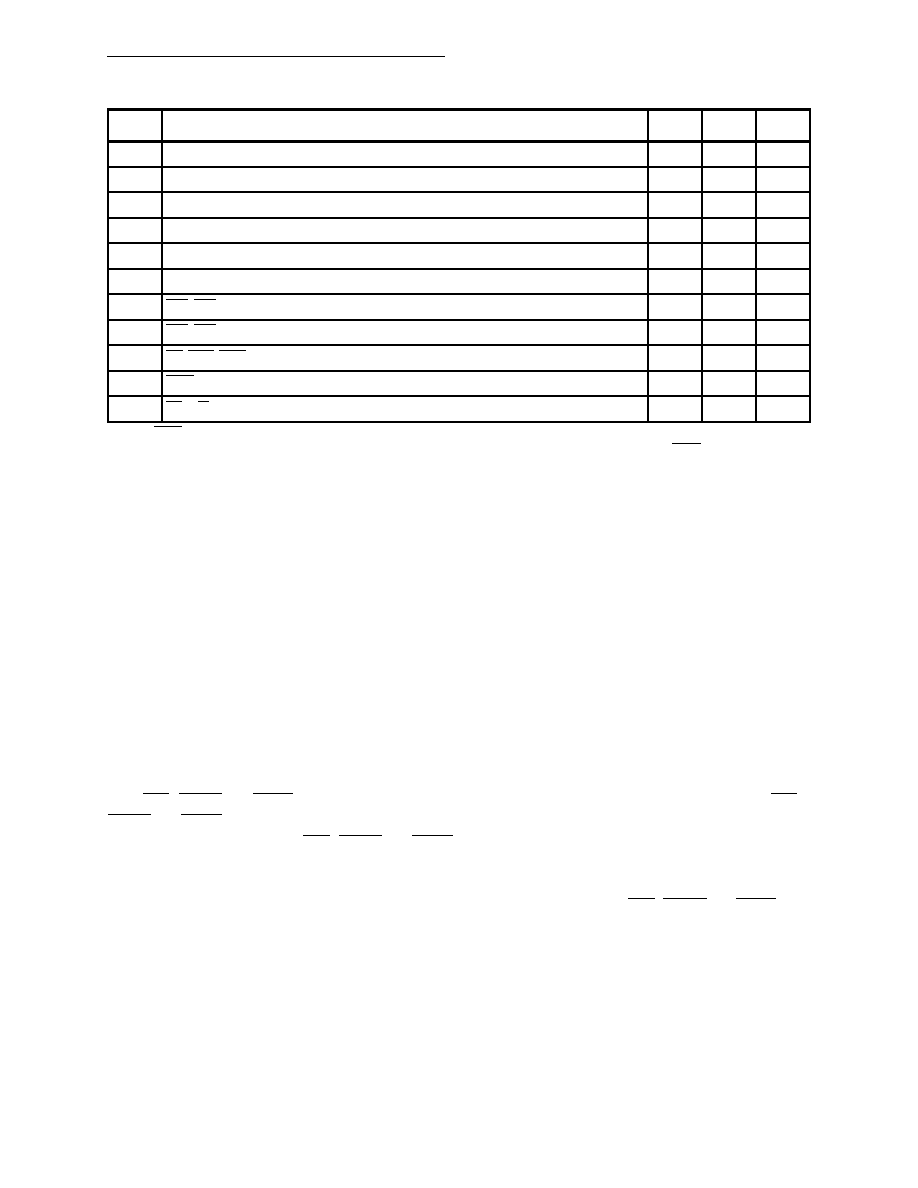
NUM
CHARACTERISTIC
MIN
MAX
UNIT
8
Address Bus Valid from CLK2, EC000 Cycle
3
30
ns
9
Address Bus Valid from CLK2, DMA Cycle
2
20
ns
10
Data Bus Driven and Valid from CLK2
2
20
ns
11
Data Bus High Impedance from CLK2
2
20
ns
12
Data Bus Setup before CLK2
2—
ns
13
Data Bus Hold after CLK2
5—
ns
14
CS7–CS0 Valid from CLK2, EC000 Cycle
3
30
ns
15
CS7–CS0 Valid from CLK2, DMA Cycle
2
20
ns
16
RD, WRL, WRU Valid from CLK2
2
20
ns
17
WAIT Asynchronous Input Hold after CLK2 *
5
—
ns
18
AS, R/W Valid from CLK2
330
ns
NOTE: WAIT is an asynchronous input and is synchronized internally by the MC68322. It requires no setup or hold time in order to be
recognized for proper operation. However, to guarantee recognition of the input at a certain edge of CLK2, WAITmust satisfy the hold
requirement.
F
re
e
sc
a
le
S
e
m
ic
o
n
d
u
c
to
r,
I
Freescale Semiconductor, Inc.
For More Information On This Product,
Go to: www.freescale.com
n
c
..
.
相關(guān)PDF資料 |
PDF描述 |
|---|---|
| MC68331CFC20B1 | 32-BIT, 20 MHz, MICROCONTROLLER, PQFP132 |
| MC68331CPV20B1 | 32-BIT, 20 MHz, MICROCONTROLLER, PQFP144 |
| MC68331CFC25B1 | 32-BIT, 25 MHz, MICROCONTROLLER, PQFP132 |
| MC68331CPV16B1 | 32-BIT, 16 MHz, MICROCONTROLLER, PQFP144 |
| MC68331CPV20 | 32-BIT, 20.97 MHz, MICROCONTROLLER, PQFP144 |
相關(guān)代理商/技術(shù)參數(shù) |
參數(shù)描述 |
|---|---|
| MC68322FT20 | 制造商:Rochester Electronics LLC 功能描述:- Bulk |
| MC68322UM | 制造商:MOTOROLA 制造商全稱:Motorola, Inc 功能描述:Integrated Printer Processor |
| MC68328 | 制造商:MOTOROLA 制造商全稱:Motorola, Inc 功能描述:Integrated Portable System Processor-DragonBall |
| MC68328P | 制造商:MOTOROLA 制造商全稱:Motorola, Inc 功能描述:Integrated Portable System Processor-DragonBall |
| MC68328UM | 制造商:MOTOROLA 制造商全稱:Motorola, Inc 功能描述:Integrated Portable System Processor-DragonBall |
發(fā)布緊急采購,3分鐘左右您將得到回復(fù)。