- 您現(xiàn)在的位置:買賣IC網(wǎng) > PDF目錄45211 > MC68322FT16 (FREESCALE SEMICONDUCTOR INC) 16-BIT, 16.667 MHz, RISC PROCESSOR, PQFP160 PDF資料下載
參數(shù)資料
| 型號: | MC68322FT16 |
| 廠商: | FREESCALE SEMICONDUCTOR INC |
| 元件分類: | 微控制器/微處理器 |
| 英文描述: | 16-BIT, 16.667 MHz, RISC PROCESSOR, PQFP160 |
| 封裝: | PLASTIC, QFP-160 |
| 文件頁數(shù): | 275/283頁 |
| 文件大小: | 1602K |
| 代理商: | MC68322FT16 |
第1頁第2頁第3頁第4頁第5頁第6頁第7頁第8頁第9頁第10頁第11頁第12頁第13頁第14頁第15頁第16頁第17頁第18頁第19頁第20頁第21頁第22頁第23頁第24頁第25頁第26頁第27頁第28頁第29頁第30頁第31頁第32頁第33頁第34頁第35頁第36頁第37頁第38頁第39頁第40頁第41頁第42頁第43頁第44頁第45頁第46頁第47頁第48頁第49頁第50頁第51頁第52頁第53頁第54頁第55頁第56頁第57頁第58頁第59頁第60頁第61頁第62頁第63頁第64頁第65頁第66頁第67頁第68頁第69頁第70頁第71頁第72頁第73頁第74頁第75頁第76頁第77頁第78頁第79頁第80頁第81頁第82頁第83頁第84頁第85頁第86頁第87頁第88頁第89頁第90頁第91頁第92頁第93頁第94頁第95頁第96頁第97頁第98頁第99頁第100頁第101頁第102頁第103頁第104頁第105頁第106頁第107頁第108頁第109頁第110頁第111頁第112頁第113頁第114頁第115頁第116頁第117頁第118頁第119頁第120頁第121頁第122頁第123頁第124頁第125頁第126頁第127頁第128頁第129頁第130頁第131頁第132頁第133頁第134頁第135頁第136頁第137頁第138頁第139頁第140頁第141頁第142頁第143頁第144頁第145頁第146頁第147頁第148頁第149頁第150頁第151頁第152頁第153頁第154頁第155頁第156頁第157頁第158頁第159頁第160頁第161頁第162頁第163頁第164頁第165頁第166頁第167頁第168頁第169頁第170頁第171頁第172頁第173頁第174頁第175頁第176頁第177頁第178頁第179頁第180頁第181頁第182頁第183頁第184頁第185頁第186頁第187頁第188頁第189頁第190頁第191頁第192頁第193頁第194頁第195頁第196頁第197頁第198頁第199頁第200頁第201頁第202頁第203頁第204頁第205頁第206頁第207頁第208頁第209頁第210頁第211頁第212頁第213頁第214頁第215頁第216頁第217頁第218頁第219頁第220頁第221頁第222頁第223頁第224頁第225頁第226頁第227頁第228頁第229頁第230頁第231頁第232頁第233頁第234頁第235頁第236頁第237頁第238頁第239頁第240頁第241頁第242頁第243頁第244頁第245頁第246頁第247頁第248頁第249頁第250頁第251頁第252頁第253頁第254頁第255頁第256頁第257頁第258頁第259頁第260頁第261頁第262頁第263頁第264頁第265頁第266頁第267頁第268頁第269頁第270頁第271頁第272頁第273頁第274頁當前第275頁第276頁第277頁第278頁第279頁第280頁第281頁第282頁第283頁
DMA Interface
8-2
MC68322 USER’S MANUAL
MOTOROLA
8.1 DMA CONFIGURATION REGISTERS
The DMA interface provides two internal memory-mapped configuration register sets called
PDMA and GDMA. These registers configure each DMA channel and provide
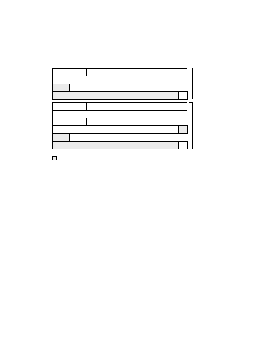
programmability for transfer address and count. Figure 8-1 illustrates the DMA interface
registers.
Figure 8-1. PDMA and GDMA Configuration Registers
8.1.1 Transfer Address Fields
The PDMA configuration register contains the PDMA DRAM transfer address field. The
GDMA configuration register contains two transfer address fields—GDMA DRAM transfer
address (GDTA) and GDMA chip-select transfer address (GCSTA). These fields define the
base address for the beginning of the transfer and they cannot be written while the BSY bit
in the active channel’s interrupt event register is set. The transfer address fields support the
entire 256M address range of the MC68322.
The GDTA field increments during a DMA transfer. For word-sized data transfers using the
GDMA channel, the transfer address is incremented after every word is transferred. When
receiving byte-sized data, the data is packed into words prior to accessing DRAM and the
address is incremented after every full word is transferred to DRAM. Likewise, for sending
byte-sized data, a word access to DRAM is made, the address in incremented, and the data
is sent unpacked as bytes to the MC68322 bus. All byte-sized data packing is organized as
big endian data.
The MC68322 bus address used for the GDMA channel is fixed and not incremented. The
transfer address for the MC68322 bus is used to access one of eight possible chip-select
banks. The GDMA chip-select transfer address appears on the output address pins of the
MC68322 bus interface (A25–A1). It is assumed the device that is connected to the banks
on the MC68322 bus used for the DMA handles any addressing issues internally.
PDMA CONFIGURATION
REGISTERS
00FFF200
00FFF202
00FFF204
00FFF206
GDMA CONFIGURATION
REGISTERS
00FFF210
00FFF212
00FFF214
00FFF216
00FFF218
00FFF21A
0000
PDMA DRAM TRANSFER ADDRESS ( HIGH WORD)
PDMA TRANSFER COUNT
GDMA TRANSFER COUNT
PDMA DRAM TRANSFER ADDRESS (LOW WORD)
0000
GDMA DRAM TRANSFER ADDRESS (HIGH WORD)
GDMA DRAM TRANSFER ADDRESS (LOW WORD)
GDMA CHIP-SELECT TRANSFER ADDRESS (HIGH WORD)
GDMA CHIP-SELECT TRANSFER ADDRESS (LOW WORD)
FR
= RESERVED
15
14
13
12
11
10
9
8
7
65432
1
0
15
14
13
12
11
10
9
8
7
65432
1
0
F
re
e
sc
a
le
S
e
m
ic
o
n
d
u
c
to
r,
I
Freescale Semiconductor, Inc.
For More Information On This Product,
Go to: www.freescale.com
n
c
..
.
相關PDF資料 |
PDF描述 |
|---|---|
| MC68331CFC20B1 | 32-BIT, 20 MHz, MICROCONTROLLER, PQFP132 |
| MC68331CPV20B1 | 32-BIT, 20 MHz, MICROCONTROLLER, PQFP144 |
| MC68331CFC25B1 | 32-BIT, 25 MHz, MICROCONTROLLER, PQFP132 |
| MC68331CPV16B1 | 32-BIT, 16 MHz, MICROCONTROLLER, PQFP144 |
| MC68331CPV20 | 32-BIT, 20.97 MHz, MICROCONTROLLER, PQFP144 |
相關代理商/技術參數(shù) |
參數(shù)描述 |
|---|---|
| MC68322FT20 | 制造商:Rochester Electronics LLC 功能描述:- Bulk |
| MC68322UM | 制造商:MOTOROLA 制造商全稱:Motorola, Inc 功能描述:Integrated Printer Processor |
| MC68328 | 制造商:MOTOROLA 制造商全稱:Motorola, Inc 功能描述:Integrated Portable System Processor-DragonBall |
| MC68328P | 制造商:MOTOROLA 制造商全稱:Motorola, Inc 功能描述:Integrated Portable System Processor-DragonBall |
| MC68328UM | 制造商:MOTOROLA 制造商全稱:Motorola, Inc 功能描述:Integrated Portable System Processor-DragonBall |
發(fā)布緊急采購,3分鐘左右您將得到回復。