- 您現(xiàn)在的位置:買賣IC網(wǎng) > PDF目錄372925 > XPC750EC XPC750P/D XPC750P RISC Microprocessor Hardware Specifications PDF資料下載
參數(shù)資料
| 型號: | XPC750EC |
| 英文描述: | XPC750P/D XPC750P RISC Microprocessor Hardware Specifications |
| 中文描述: | XPC750P /數(shù)XPC750P RISC微處理器硬件規(guī)格 |
| 文件頁數(shù): | 19/52頁 |
| 文件大小: | 1274K |
| 代理商: | XPC750EC |
第1頁第2頁第3頁第4頁第5頁第6頁第7頁第8頁第9頁第10頁第11頁第12頁第13頁第14頁第15頁第16頁第17頁第18頁當(dāng)前第19頁第20頁第21頁第22頁第23頁第24頁第25頁第26頁第27頁第28頁第29頁第30頁第31頁第32頁第33頁第34頁第35頁第36頁第37頁第38頁第39頁第40頁第41頁第42頁第43頁第44頁第45頁第46頁第47頁第48頁第49頁第50頁第51頁第52頁
MOTOROLA
MPC755 RISC Microprocessor Hardware Specifications
19
Electrical and Thermal Characteristics
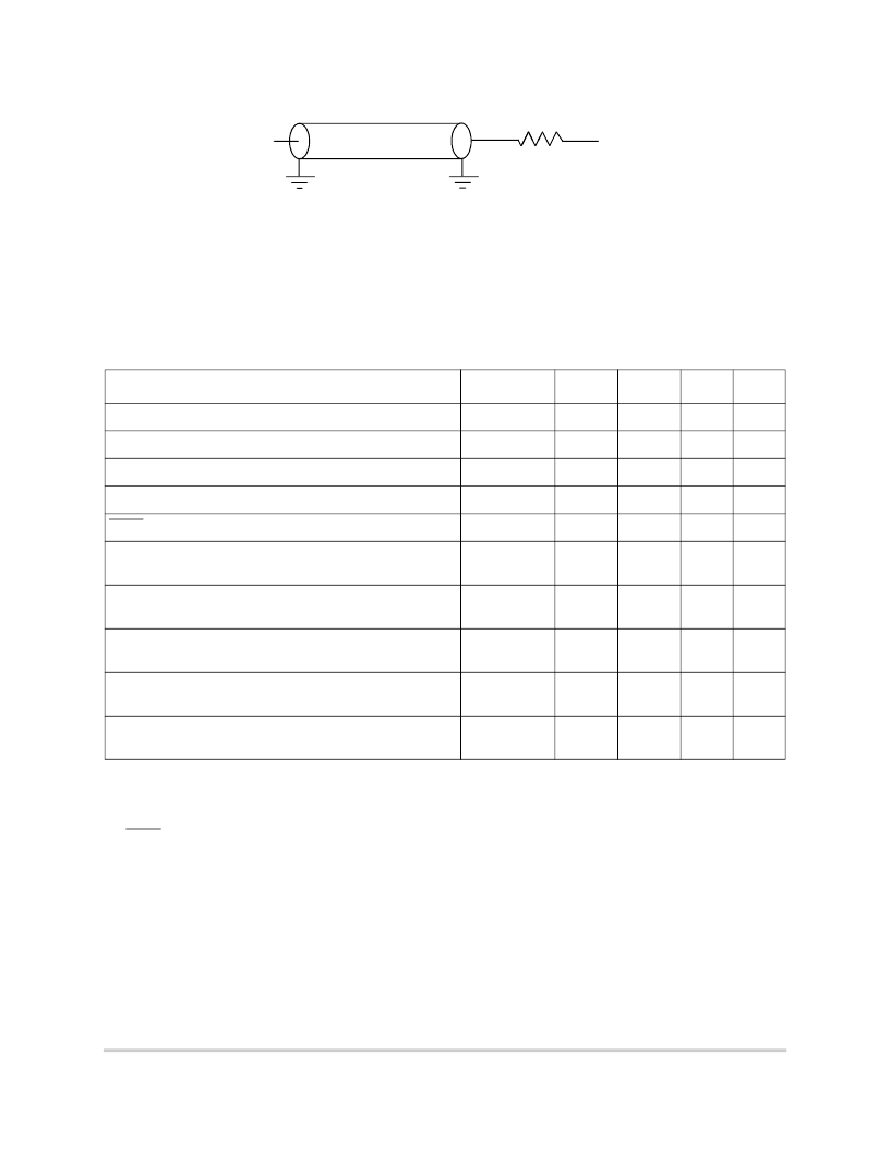
Figure 10 provides the AC test load for L2 interface of the MPC755.
Figure 10. AC Test Load for the L2 Interface
1.4.2.5
IEEE 1149.1 AC Timing Specifications
Table 13 provides the IEEE 1149.1 (JTAG) AC timing specifications as defined in Figure 12, Figure 13,
Figure 14, and Figure 15.
Table 13. JTAG AC Timing Specifications (Independent of SYSCLK)
1
At recommended operating conditions (see Table 3)
Parameter
Symbol
Min
Max
Unit
Notes
TCK frequency of operation
f
TCLK
0
16
MHz
TCK cycle time
t
TCLK
62.5
—
ns
TCK clock pulse width measured at 1.4 V
t
JHJL
31
—
ns
TCK rise and fall times
t
JR
, t
JF
0
2
ns
TRST assert time
t
TRST
25
—
ns
2
Input setup times:
Boundary-scan data
TMS, TDI
t
DVJH
t
IVJH
4
0
—
—
ns
3
Input hold times:
Boundary-scan data
TMS, TDI
t
DXJH
t
IXJH
15
12
—
—
ns
3
Valid times:
Boundary-scan data
TDO
t
JLDV
t
JLOV
—
—
4
4
ns
4
Output hold times:
Boundary-scan data
TDO
t
JLDH
t
JLOH
25
12
—
—
ns
4
TCK to output high impedance:
Boundary-scan data
TDO
t
JLDZ
t
JLOZ
3
3
19
9
ns
4, 5
Notes:
1. All outputs are measured from the midpoint voltage of the falling/rising edge of TCLK to the midpoint of the signal
in question. The output timings are measured at the pins. All output timings assume a purely resistive 50-
load
(see Figure 11). Time-of-flight delays must be added for trace lengths, vias, and connectors in the system.
2. TRST is an asynchronous level sensitive signal which must be asserted for this minimum time to be recognized.
3. Non-JTAG signal input timing with respect to TCK.
4. Non-JTAG signal output timing with respect to TCK.
5. Guaranteed by design and characterization.
Output
Z
0
= 50
L2OV
DD
/2
R
L
= 50
相關(guān)PDF資料 |
PDF描述 |
|---|---|
| XPC801ZP25 | Microprocessor |
| XPC801ZP40 | Microprocessor |
| XPC821ZP40 | Microprocessor |
| XPC823ZP25 | Microprocessor |
| XPC823ZP50 | Microprocessor |
相關(guān)代理商/技術(shù)參數(shù) |
參數(shù)描述 |
|---|---|
| XPC755BPX300LD | 制造商:未知廠家 制造商全稱:未知廠家 功能描述:Microprocessor |
| XPC755BPX350LD | 制造商:未知廠家 制造商全稱:未知廠家 功能描述:Microprocessor |
| XPC755BPX400LD | 制造商:未知廠家 制造商全稱:未知廠家 功能描述:Microprocessor |
| XPC755BPX400LE | 制造商:Freescale Semiconductor 功能描述: |
| XPC755BRX300LD | 制造商:未知廠家 制造商全稱:未知廠家 功能描述:Microprocessor |
發(fā)布緊急采購,3分鐘左右您將得到回復(fù)。