- 您現(xiàn)在的位置:買賣IC網(wǎng) > PDF目錄372925 > XPC750EC XPC750P/D XPC750P RISC Microprocessor Hardware Specifications PDF資料下載
參數(shù)資料
| 型號(hào): | XPC750EC |
| 英文描述: | XPC750P/D XPC750P RISC Microprocessor Hardware Specifications |
| 中文描述: | XPC750P /數(shù)XPC750P RISC微處理器硬件規(guī)格 |
| 文件頁數(shù): | 7/52頁 |
| 文件大小: | 1274K |
| 代理商: | XPC750EC |
第1頁第2頁第3頁第4頁第5頁第6頁當(dāng)前第7頁第8頁第9頁第10頁第11頁第12頁第13頁第14頁第15頁第16頁第17頁第18頁第19頁第20頁第21頁第22頁第23頁第24頁第25頁第26頁第27頁第28頁第29頁第30頁第31頁第32頁第33頁第34頁第35頁第36頁第37頁第38頁第39頁第40頁第41頁第42頁第43頁第44頁第45頁第46頁第47頁第48頁第49頁第50頁第51頁第52頁
MOTOROLA
MPC755 RISC Microprocessor Hardware Specifications
7
Electrical and Thermal Characteristics
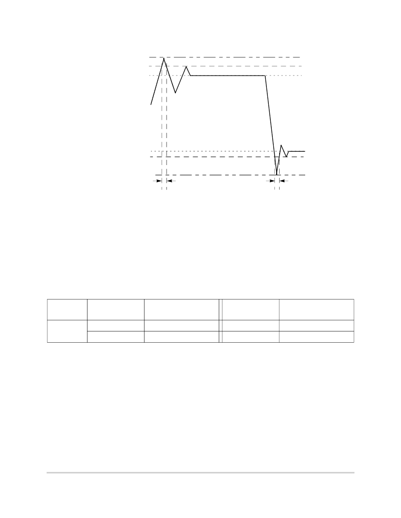
Figure 2 shows the allowable undershoot and overshoot voltage on the MPC755.
Figure 2. Overshoot/Undershoot Voltage
The MPC755 provides several I/O voltages to support both compatibility with existing systems and
migration to future systems. The MPC755 core voltage must always be provided at nominal 2.0 V (see
Table 3 for actual recommended core voltage). Voltage to the L2 I/Os and processor interface I/Os are
provided through separate sets of supply pins and may be provided at the voltages shown in Table 2. The
input voltage threshold for each bus is selected by sampling the state of the voltage select pins BVSEL and
L2VSEL during operation. These signals must remain stable during part operation and cannot change. The
output voltage will swing from GND to the maximum voltage applied to the OV
DD
or L2OV
DD
power pins.
Table 2 describes the input threshold voltage setting.
Table 2. Input Threshold Voltage Setting
Part
Revision
BVSEL Signal
Processor Bus
Interface Voltage
L2VSEL Signal
L2 Bus
Interface Voltage
E
0
Not Available
0
Not Available
1
2.5 V / 3.3 V
1
2.5 V / 3.3 V
Caution:
The input threshold selection must agree with the OV
DD
/L2OV
DD
voltages supplied.
Note:
The input threshold settings above are different for all revisions prior to Rev. 2.8 (Rev. E). For more
information, refer to Section 1.10.2, “Part Numbers Not Fully Addressed by This Document.”
V
IH
GND
GND – 0.3 V
GND – 0.7 V
Not to Exceed 10%
of t
SYSCLK
(L2)OV
DD
+ 20%
(L2)OV
DD
+ 5%
V
IL
(L2)OV
DD
相關(guān)PDF資料 |
PDF描述 |
|---|---|
| XPC801ZP25 | Microprocessor |
| XPC801ZP40 | Microprocessor |
| XPC821ZP40 | Microprocessor |
| XPC823ZP25 | Microprocessor |
| XPC823ZP50 | Microprocessor |
相關(guān)代理商/技術(shù)參數(shù) |
參數(shù)描述 |
|---|---|
| XPC755BPX300LD | 制造商:未知廠家 制造商全稱:未知廠家 功能描述:Microprocessor |
| XPC755BPX350LD | 制造商:未知廠家 制造商全稱:未知廠家 功能描述:Microprocessor |
| XPC755BPX400LD | 制造商:未知廠家 制造商全稱:未知廠家 功能描述:Microprocessor |
| XPC755BPX400LE | 制造商:Freescale Semiconductor 功能描述: |
| XPC755BRX300LD | 制造商:未知廠家 制造商全稱:未知廠家 功能描述:Microprocessor |
發(fā)布緊急采購,3分鐘左右您將得到回復(fù)。