- 您現(xiàn)在的位置:買賣IC網(wǎng) > PDF目錄295887 > EP2C20F256I6N (ALTERA CORP) FPGA, 1196 CLBS, PBGA256 PDF資料下載
參數(shù)資料
| 型號: | EP2C20F256I6N |
| 廠商: | ALTERA CORP |
| 元件分類: | FPGA |
| 英文描述: | FPGA, 1196 CLBS, PBGA256 |
| 封裝: | LEAD FREE, FBGA-256 |
| 文件頁數(shù): | 63/168頁 |
| 文件大小: | 2206K |
| 代理商: | EP2C20F256I6N |
第1頁第2頁第3頁第4頁第5頁第6頁第7頁第8頁第9頁第10頁第11頁第12頁第13頁第14頁第15頁第16頁第17頁第18頁第19頁第20頁第21頁第22頁第23頁第24頁第25頁第26頁第27頁第28頁第29頁第30頁第31頁第32頁第33頁第34頁第35頁第36頁第37頁第38頁第39頁第40頁第41頁第42頁第43頁第44頁第45頁第46頁第47頁第48頁第49頁第50頁第51頁第52頁第53頁第54頁第55頁第56頁第57頁第58頁第59頁第60頁第61頁第62頁當(dāng)前第63頁第64頁第65頁第66頁第67頁第68頁第69頁第70頁第71頁第72頁第73頁第74頁第75頁第76頁第77頁第78頁第79頁第80頁第81頁第82頁第83頁第84頁第85頁第86頁第87頁第88頁第89頁第90頁第91頁第92頁第93頁第94頁第95頁第96頁第97頁第98頁第99頁第100頁第101頁第102頁第103頁第104頁第105頁第106頁第107頁第108頁第109頁第110頁第111頁第112頁第113頁第114頁第115頁第116頁第117頁第118頁第119頁第120頁第121頁第122頁第123頁第124頁第125頁第126頁第127頁第128頁第129頁第130頁第131頁第132頁第133頁第134頁第135頁第136頁第137頁第138頁第139頁第140頁第141頁第142頁第143頁第144頁第145頁第146頁第147頁第148頁第149頁第150頁第151頁第152頁第153頁第154頁第155頁第156頁第157頁第158頁第159頁第160頁第161頁第162頁第163頁第164頁第165頁第166頁第167頁第168頁
Altera Corporation
5–65
February 2008
Cyclone II Device Handbook, Volume 1
DC Characteristics and Timing Specifications
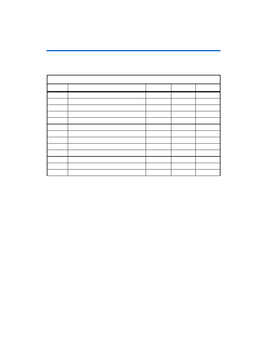
Table 5–53 shows the JTAG timing parameters and values for Cyclone II
devices.
1
Cyclone II devices must be within the first 17 devices in a JTAG
chain. All of these devices have the same JTAG controller. If any
of the Cyclone II devices are in the 18th position or after they will
fail configuration. This does not affect the SignalTap II logic
analyzer.
f
For more information on JTAG, refer to the IEEE 1149.1 (JTAG)
Boundary-Scan Testing for Cyclone II Devices chapter in the Cyclone II
Handbook.
Table 5–53. Cyclone II JTAG Timing Parameters and Values
Symbol
Parameter
Min
Max
Unit
tJCP
TCK clock period
40
—
ns
tJCH
TCK clock high time
20
—
ns
tJCL
TCK clock low time
20
—
ns
tJPSU
JTAG port setup time (2)
5—
ns
tJPH
JTAG port hold time
10
—
ns
tJPCO
JTAG port clock to output (2)
—13
ns
tJPZX
JTAG port high impedance to valid output (2)
—13
ns
tJPXZ
JTAG port valid output to high impedance (2)
—13
ns
tJSSU
Capture register setup time (2)
5—
ns
tJSH
Capture register hold time
10
—
ns
tJSCO
Update register clock to output
—
25
ns
tJSZX
Update register high impedance to valid output
—
25
ns
tJSXZ
Update register valid output to high impedance
—
25
ns
Notes to Table 5–53:
(1)
This information is preliminary.
(2)
This specification is shown for 3.3-V LVTTL/LVCMOS and 2.5-V LVTTL/LVCMOS operation of the JTAG pins. For
1.8-V LVTTL/LVCMOS and 1.5-V LVCMOS, the JTAG port and capture register clock setup time is 3 ns and port
clock to output time is 15 ns.
相關(guān)PDF資料 |
PDF描述 |
|---|---|
| EP2SGX60CF780C3N | FPGA, 60440 CLBS, 717 MHz, PBGA780 |
| EP2SGX60CF780C3 | FPGA, 60440 CLBS, 717 MHz, PBGA780 |
| EP2SGX60CF780C4N | FPGA, 60440 CLBS, 717 MHz, PBGA780 |
| EP2SGX60CF780C4 | FPGA, 60440 CLBS, 717 MHz, PBGA780 |
| EP2SGX60CF780C5N | FPGA, 60440 CLBS, 640 MHz, PBGA780 |
相關(guān)代理商/技術(shù)參數(shù) |
參數(shù)描述 |
|---|---|
| EP2C20F256I8 | 功能描述:FPGA - 現(xiàn)場可編程門陣列 FPGA - Cyclone II 1172 LABs 152 IOs RoHS:否 制造商:Altera Corporation 系列:Cyclone V E 柵極數(shù)量: 邏輯塊數(shù)量:943 內(nèi)嵌式塊RAM - EBR:1956 kbit 輸入/輸出端數(shù)量:128 最大工作頻率:800 MHz 工作電源電壓:1.1 V 最大工作溫度:+ 70 C 安裝風(fēng)格:SMD/SMT 封裝 / 箱體:FBGA-256 |
| EP2C20F256I8GA | 制造商:Altera Corporation 功能描述: |
| EP2C20F256I8N | 功能描述:FPGA - 現(xiàn)場可編程門陣列 FPGA - Cyclone II 1172 LABs 152 IOs RoHS:否 制造商:Altera Corporation 系列:Cyclone V E 柵極數(shù)量: 邏輯塊數(shù)量:943 內(nèi)嵌式塊RAM - EBR:1956 kbit 輸入/輸出端數(shù)量:128 最大工作頻率:800 MHz 工作電源電壓:1.1 V 最大工作溫度:+ 70 C 安裝風(fēng)格:SMD/SMT 封裝 / 箱體:FBGA-256 |
| EP2C20F484C6 | 功能描述:FPGA - 現(xiàn)場可編程門陣列 FPGA - Cyclone II 1172 LABs 315 IOs RoHS:否 制造商:Altera Corporation 系列:Cyclone V E 柵極數(shù)量: 邏輯塊數(shù)量:943 內(nèi)嵌式塊RAM - EBR:1956 kbit 輸入/輸出端數(shù)量:128 最大工作頻率:800 MHz 工作電源電壓:1.1 V 最大工作溫度:+ 70 C 安裝風(fēng)格:SMD/SMT 封裝 / 箱體:FBGA-256 |
| EP2C20F484C6N | 功能描述:FPGA - 現(xiàn)場可編程門陣列 FPGA - Cyclone II 1172 LABs 315 IOs RoHS:否 制造商:Altera Corporation 系列:Cyclone V E 柵極數(shù)量: 邏輯塊數(shù)量:943 內(nèi)嵌式塊RAM - EBR:1956 kbit 輸入/輸出端數(shù)量:128 最大工作頻率:800 MHz 工作電源電壓:1.1 V 最大工作溫度:+ 70 C 安裝風(fēng)格:SMD/SMT 封裝 / 箱體:FBGA-256 |
發(fā)布緊急采購,3分鐘左右您將得到回復(fù)。