- 您現(xiàn)在的位置:買賣IC網(wǎng) > PDF目錄224505 > MT29F4G08BABWP 512M X 8 FLASH 2.7V PROM, 18 ns, PDSO48 PDF資料下載
參數(shù)資料
| 型號: | MT29F4G08BABWP |
| 元件分類: | PROM |
| 英文描述: | 512M X 8 FLASH 2.7V PROM, 18 ns, PDSO48 |
| 封裝: | LEAD FREE, TSOP1-48 |
| 文件頁數(shù): | 17/57頁 |
| 文件大?。?/td> | 1057K |
| 代理商: | MT29F4G08BABWP |
第1頁第2頁第3頁第4頁第5頁第6頁第7頁第8頁第9頁第10頁第11頁第12頁第13頁第14頁第15頁第16頁當(dāng)前第17頁第18頁第19頁第20頁第21頁第22頁第23頁第24頁第25頁第26頁第27頁第28頁第29頁第30頁第31頁第32頁第33頁第34頁第35頁第36頁第37頁第38頁第39頁第40頁第41頁第42頁第43頁第44頁第45頁第46頁第47頁第48頁第49頁第50頁第51頁第52頁第53頁第54頁第55頁第56頁第57頁
PDF: 09005aef818a56a7 / Source: 09005aef81590bdd
Micron Technology, Inc., reserves the right to change products or specifications without notice.
2gb_nand_m29b__2.fm - Rev. I 1/06 EN
24
2004 Micron Technology, Inc. All rights reserved.
2, 4, 8Gb: x8/x16 Multiplexed NAND Flash Memory
Command Definitions
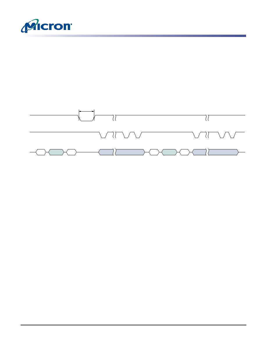
RANDOM DATA READ 05h-E0h
The RANDOM DATA READ command enables the user to specify a new column address
so the data at single or multiple addresses can be read. The random read mode is
enabled after a normal PAGE READ (00h-30h sequence).
Random data can be output after the initial page read by writing an 05h-E0h command
sequence along with the new column address (two cycles).
The RANDOM DATA READ command can be issued without limit within the page.
Only data on the current page can be read. Pulsing the RE# pin outputs data sequen-
tially. See Figure 19 on page 24.
Figure 19:
RANDOM DATA READ Operation
PAGE READ CACHE MODE START 31h; PAGE READ CACHE MODE START LAST 3Fh
Micron NAND Flash devices have a cache register that can be used to increase READ
operation speed when accessing sequential pages in a block.
First, a normal PAGE READ (00h-30h) command sequence is issued. (See Figure 20 on
to transfer the first page of data from the memory to the data register. After R/B# returns
to HIGH, the PAGE READ CACHE MODE START (31h) command is latched into the
command register. R/B# goes LOW for tDCBSYR1 while data is being transferred from
the data register to the cache register. Once the data register contents are transferred to
the cache register, another PAGE READ is automatically started as part of the 31h com-
mand. Data is transferred from the next sequential page of the memory array to the data
register during the same time data is being read serially (pulsing of RE#) from the cache
register. If the total time to output data exceeds tR, then the PAGE READ is hidden.
The second and subsequent pages of data are transferred to the cache register by issuing
additional 31h commands. R/B# will stay LOW up to tDCBSYR2. This time can vary,
depending on whether the previous memory-to-data-register transfer was completed
prior to issuing the next 31h command. If the data transfer from memory to the data reg-
ister is not completed before the 31h command is issued, R/B# stays LOW until the
transfer is complete.
It is not necessary to output a whole page of data before issuing another 31h command.
R/B# will stay LOW until the previous PAGE READ is complete and the data has been
transferred to the cache register.
To read out the last page of data, the PAGE READ CACHE MODE START LAST (3Fh)
command is issued. This command transfers data from the data register to the cache
register without issuing another PAGE READ. (See Figure 20 on page 25.)
RE#
I/Ox
00h
Address
(5 Cycles)
Data Output
30h
05h
Address
(2 Cycles)
E0h
R/B#
tR
相關(guān)PDF資料 |
PDF描述 |
|---|---|
| MT36JSZF51272PDY-1G6XX | 512M X 72 DDR DRAM MODULE, DMA240 |
| MT3S04AU | UHF BAND, Si, NPN, RF SMALL SIGNAL TRANSISTOR |
| MT41J512M4JE-187EIT:A | 64M X 4 DDR DRAM, PBGA82 |
| MT42C8255RG-7TR | 256K X 8 VIDEO DRAM, 70 ns, PDSO40 |
| MT46V32M16TG-75ELIT | 32M X 16 DDR DRAM, 0.75 ns, PDSO66 |
相關(guān)代理商/技術(shù)參數(shù) |
參數(shù)描述 |
|---|---|
| MT29F4G08BABWP-ET | 功能描述:IC FLASH 4GBIT 48TSOP RoHS:是 類別:集成電路 (IC) >> 存儲器 系列:- 標準包裝:1 系列:- 格式 - 存儲器:RAM 存儲器類型:SDRAM 存儲容量:256M(8Mx32) 速度:143MHz 接口:并聯(lián) 電源電壓:3 V ~ 3.6 V 工作溫度:-40°C ~ 85°C 封裝/外殼:90-VFBGA 供應(yīng)商設(shè)備封裝:90-VFBGA(8x13) 包裝:托盤 其它名稱:Q2841869 |
| MT29F4G08BABWP-ET TR | 功能描述:IC FLASH 4GBIT 48TSOP RoHS:是 類別:集成電路 (IC) >> 存儲器 系列:- 標準包裝:1 系列:- 格式 - 存儲器:RAM 存儲器類型:SDRAM 存儲容量:256M(8Mx32) 速度:143MHz 接口:并聯(lián) 電源電壓:3 V ~ 3.6 V 工作溫度:-40°C ~ 85°C 封裝/外殼:90-VFBGA 供應(yīng)商設(shè)備封裝:90-VFBGA(8x13) 包裝:托盤 其它名稱:Q2841869 |
| MT29F4G08BBBWP | 功能描述:IC FLASH 4GBIT 48TSOP RoHS:是 類別:集成電路 (IC) >> 存儲器 系列:- 標準包裝:1 系列:- 格式 - 存儲器:RAM 存儲器類型:SDRAM 存儲容量:256M(8Mx32) 速度:143MHz 接口:并聯(lián) 電源電壓:3 V ~ 3.6 V 工作溫度:-40°C ~ 85°C 封裝/外殼:90-VFBGA 供應(yīng)商設(shè)備封裝:90-VFBGA(8x13) 包裝:托盤 其它名稱:Q2841869 |
發(fā)布緊急采購,3分鐘左右您將得到回復(fù)。