- 您現(xiàn)在的位置:買賣IC網(wǎng) > PDF目錄98254 > TLV320AIC36IZQE (TEXAS INSTRUMENTS INC) SPECIALTY CONSUMER CIRCUIT, PBGA80 PDF資料下載
參數(shù)資料
| 型號: | TLV320AIC36IZQE |
| 廠商: | TEXAS INSTRUMENTS INC |
| 元件分類: | 消費家電 |
| 英文描述: | SPECIALTY CONSUMER CIRCUIT, PBGA80 |
| 封裝: | 5 X 5 MM, GREEN, PLASTIC, VFBGA-80 |
| 文件頁數(shù): | 112/165頁 |
| 文件大小: | 1895K |
| 代理商: | TLV320AIC36IZQE |
第1頁第2頁第3頁第4頁第5頁第6頁第7頁第8頁第9頁第10頁第11頁第12頁第13頁第14頁第15頁第16頁第17頁第18頁第19頁第20頁第21頁第22頁第23頁第24頁第25頁第26頁第27頁第28頁第29頁第30頁第31頁第32頁第33頁第34頁第35頁第36頁第37頁第38頁第39頁第40頁第41頁第42頁第43頁第44頁第45頁第46頁第47頁第48頁第49頁第50頁第51頁第52頁第53頁第54頁第55頁第56頁第57頁第58頁第59頁第60頁第61頁第62頁第63頁第64頁第65頁第66頁第67頁第68頁第69頁第70頁第71頁第72頁第73頁第74頁第75頁第76頁第77頁第78頁第79頁第80頁第81頁第82頁第83頁第84頁第85頁第86頁第87頁第88頁第89頁第90頁第91頁第92頁第93頁第94頁第95頁第96頁第97頁第98頁第99頁第100頁第101頁第102頁第103頁第104頁第105頁第106頁第107頁第108頁第109頁第110頁第111頁當前第112頁第113頁第114頁第115頁第116頁第117頁第118頁第119頁第120頁第121頁第122頁第123頁第124頁第125頁第126頁第127頁第128頁第129頁第130頁第131頁第132頁第133頁第134頁第135頁第136頁第137頁第138頁第139頁第140頁第141頁第142頁第143頁第144頁第145頁第146頁第147頁第148頁第149頁第150頁第151頁第152頁第153頁第154頁第155頁第156頁第157頁第158頁第159頁第160頁第161頁第162頁第163頁第164頁第165頁
SBAS387A – MAY 2009 – REVISED JUNE 2010
www.ti.com
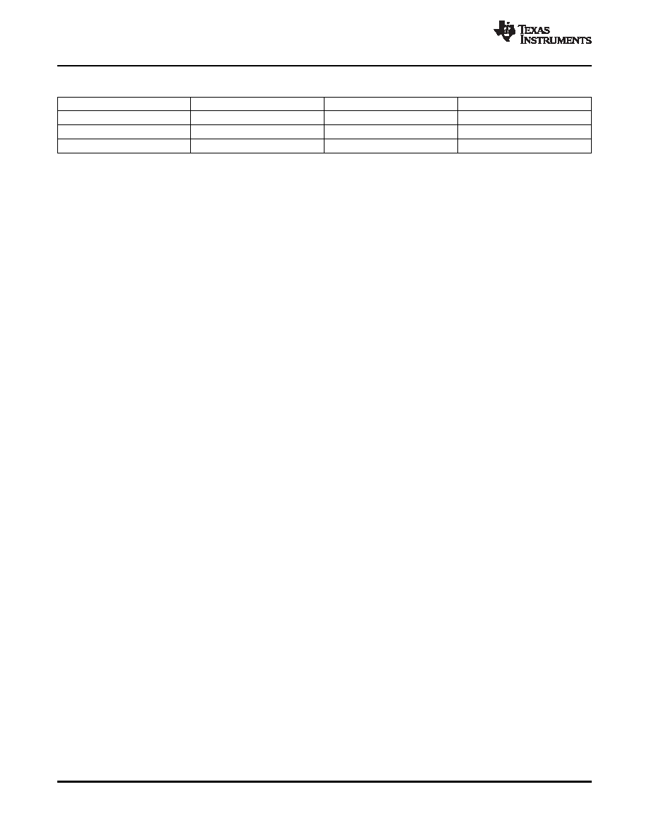
Table 5-17. DAC Interpolation Filter C, Specification
Parameter
Condition
Value (Typical)
Units
Filter gain pass band
0 … 0.35 Fs
±0.03
dB
Filter gain stop band
0.60 … 1.4 Fs
–43
dB
Filter group delay
13/Fs
s
5.12 DAC Output Drivers
5.12.1 Analog Fully Differential Line Output Drivers
The TLV320AIC36 has two fully differential line output drivers, each capable of driving a 10k
differential
load. Each driver can connect to the left or the right DAC, the left or the right ADC PGA output, the left or
right line input, or any combination of the six. The design includes extensive capability to adjust signal
levels independently before any mixing occurs, beyond that already provided by the PGA gain and the
DAC digital volume control. Note that since both left and right channel signals are routed to all output
drivers, a mono mix of any of the stereo signals can easily be obtained by setting the volume controls of
both left and right channel signals to –6 dB and mixing them. Undesired signals can also be disconnected
from the mix as well through register control.
The TLV320AIC36 includes an output level control on each output driver with limited gain adjustment from
0 dB to +9 dB. The output driver circuitry in this device are designed to provide a low distortion output
while playing full-scale stereo DAC signals at a 0 dB gain setting. However, a higher amplitude output can
be obtained at the cost of increased signal distortion at the output. This output level control allows the user
to make this tradeoff based on the requirements of the end equipment. Note that this output level control
is not intended to be used as a standard output volume control. It is expected to be used only sparingly for
level setting, that is, adjustment of the full-scale output range of the device.
Each differential line output driver can be powered down independently of the others when it is not needed
in the system. When placed into powerdown through register programming, the driver output pins will be
placed into a high-Z, high-impedance state.
The signal routing for the line level drivers is configured using Page 2, Registers 80 through 93
5.12.2 Analog High-Power Output Drivers
The TLV320AIC36 includes four single-ended high power output drivers arranged as two stereo pairs.
These output drivers are capable of driving 0.89 Vrms each into a 16-
load if one pair is enabled or 0.5
Vrms each into 16-
if both pairs are enabled. The volume control and mixing blocks for the high-power
output drivers are effectively identical to those of the line-level drivers. Note that each of these drivers
have a output level control block like those included with the line output drivers, allowing gain adjustment
up to +9 dB on the output signal. As in the previous case, this output level adjustment is not intended to
be used as a standard volume control, but instead is included for additional full-scale output signal level
control. In order to drive 0.89 Vrms for a full-scale DAC output into the load, the output level adjustment
must be set to +2 dB.
The high power output drivers include additional circuitry to avoid artifacts on the audio output during
power-on and power-off transient conditions. The power-up delay time for the high power output drivers is
programmable over a wide range of time delays, from instantaneous up to 4-sec, using Page-2/Reg-42.
When these output drivers are powered down, they can be placed into a variety of output conditions based
on register programming. If lowest power operation is desired, then the outputs can be placed into a
tri-state condition, and all power to the output stage is removed. However, this generally results in the
output nodes drifting to rest near the upper or lower analog supply, due to small leakage currents at the
pins. This then results in a longer delay requirement to avoid output artifacts during driver power-on. In
order to reduce this required power-on delay, the TLV320AIC36 includes an option for the output pins of
the drivers to be weakly driven to the AGND level they would normally rest at when powered with no
signal applied.
50
APPLICATION INFORMATION
Copyright 2009–2010, Texas Instruments Incorporated
Product Folder Link(s): TLV320AIC36
相關PDF資料 |
PDF描述 |
|---|---|
| TLV320DAC23IPW | SERIAL INPUT LOADING, 32-BIT DAC, PDSO28 |
| TLV320DAC23IGQER | SERIAL INPUT LOADING, 32-BIT DAC, PBGA80 |
| TLV320DAC23PWR | SERIAL INPUT LOADING, 32-BIT DAC, PDSO28 |
| TLV320DAC23RHDR | SERIAL INPUT LOADING, 32-BIT DAC, PQCC28 |
| TLV320DAC23RHDG4 | SERIAL INPUT LOADING, 32-BIT DAC, PQCC28 |
相關代理商/技術參數(shù) |
參數(shù)描述 |
|---|---|
| TLV320AIC36IZQER | 功能描述:接口—CODEC Low Pwr Stereo Aud Codec RoHS:否 制造商:Texas Instruments 類型: 分辨率: 轉(zhuǎn)換速率:48 kSPs 接口類型:I2C ADC 數(shù)量:2 DAC 數(shù)量:4 工作電源電壓:1.8 V, 2.1 V, 2.3 V to 5.5 V 最大工作溫度:+ 85 C 安裝風格:SMD/SMT 封裝 / 箱體:DSBGA-81 封裝:Reel |
| TLV320ALC23 | 制造商:TI 制造商全稱:Texas Instruments 功能描述:Evaluation Platform for the TLV320ALC23 Stereo Audio CODEC and TLV230DAC23 Stereo DAC |
| TLV320ALC31 | 制造商:BB 制造商全稱:BB 功能描述:LOW POWER STEREO AUDIO CODEC FOR PORTABLE AUDIO/TELEPHONY |
| TLV320DA26IRHBG4 | 功能描述:音頻數(shù)/模轉(zhuǎn)換器 IC Lo-Pwr Ster DAC w/Hdphn/Spkr Amp RoHS:否 制造商:Texas Instruments 轉(zhuǎn)換器數(shù)量: 分辨率:16 bit 接口類型:I2S, UBS 轉(zhuǎn)換速率: 信噪比:98 dB 工作電源電壓:5 V DAC 輸出端數(shù)量:2 工作溫度范圍:- 25 C to + 85 C 電源電流:23 mA 安裝風格:SMD/SMT 封裝 / 箱體:TQFP-32 封裝:Reel |
| TLV320DAC23 | 制造商:TI 制造商全稱:Texas Instruments 功能描述:STEREO AUDIO D/A CONVERTER, 8-TO 96KHZ WITH INTERGRATED HEADPHONE AMPLIFIER |
發(fā)布緊急采購,3分鐘左右您將得到回復。