- 您現(xiàn)在的位置:買賣IC網(wǎng) > PDF目錄373200 > KU386 (Intel Corp.) SX MICROPROCESSOR PDF資料下載
參數(shù)資料
| 型號: | KU386 |
| 廠商: | Intel Corp. |
| 英文描述: | SX MICROPROCESSOR |
| 中文描述: | SX微處理器 |
| 文件頁數(shù): | 4/102頁 |
| 文件大小: | 1268K |
| 代理商: | KU386 |
第1頁第2頁第3頁當前第4頁第5頁第6頁第7頁第8頁第9頁第10頁第11頁第12頁第13頁第14頁第15頁第16頁第17頁第18頁第19頁第20頁第21頁第22頁第23頁第24頁第25頁第26頁第27頁第28頁第29頁第30頁第31頁第32頁第33頁第34頁第35頁第36頁第37頁第38頁第39頁第40頁第41頁第42頁第43頁第44頁第45頁第46頁第47頁第48頁第49頁第50頁第51頁第52頁第53頁第54頁第55頁第56頁第57頁第58頁第59頁第60頁第61頁第62頁第63頁第64頁第65頁第66頁第67頁第68頁第69頁第70頁第71頁第72頁第73頁第74頁第75頁第76頁第77頁第78頁第79頁第80頁第81頁第82頁第83頁第84頁第85頁第86頁第87頁第88頁第89頁第90頁第91頁第92頁第93頁第94頁第95頁第96頁第97頁第98頁第99頁第100頁第101頁第102頁
Intel386
TM
SX MICROPROCESSOR
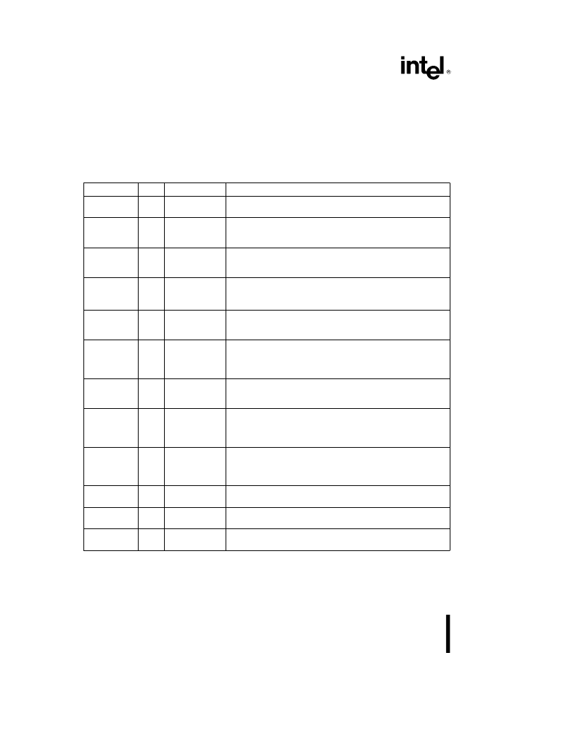
1.0 PIN DESCRIPTION
(Continued)
The following are the Intel386
TM
SX Microprocessor pin descriptions. The following definitions are used in the
pin descriptions:
Y
I
O
I/O
-
The named signal is active LOW.
Input signal.
Output signal.
Input and Output signal.
No electrical connection.
Symbol
Type
Pin
Name and Function
CLK2
I
15
CLK2
provides the fundamental timing for the Intel386 SX
Microprocessor. For additional information see
Clock.
RESET
I
33
RESET
suspends any operation in progress and places the
Intel386 SX Microprocessor in a known reset state. See
Interrupt Signals
for additional information.
D
15
–D
0
I/O
81-83,86-90,
92-96,99-100,1
Data Bus
inputs data during memory, I/O and interrupt
acknowledge read cycles and outputs data during memory and
I/O write cycles. See
Data Bus
for additional information.
A
23
–A
1
O
80-79,76-72,70,
66-64,62-58,
56-51,18
Address Bus
outputs physical memory or port I/O addresses.
See
Address Bus
for additional information.
W/R
Y
O
25
Write/Read
is a bus cycle definition pin that distinguishes write
cycles from read cycles. See
Bus Cycle Definition Signals
for
additional information.
D/C
Y
O
24
Data/Control
is a bus cycle definition pin that distinguishes data
cycles, either memory or I/O, from control cycles which are:
interrupt acknowledge, halt, and code fetch. See
Bus Cycle
Definition Signals
for additional information.
M/IO
Y
O
23
Memory/IO
is a bus cycle definition pin that distinguishes
memory cycles from input/output cycles. See
Bus Cycle
Definition Signals
for additional information.
LOCK
Y
O
26
Bus Lock
is a bus cycle definition pin that indicates that other
system bus masters are not to gain control of the system bus
while it is active. See
Bus Cycle Definition Signals
for
additional information.
ADS
Y
O
16
Address Status
indicates that a valid bus cycle definition and
address (W/R
Y
, D/C
Y
, M/IO
Y
, BHE
Y
, BLE
Y
and A
23
–A
1
are
being driven at the Intel386 SX Microprocessor pins. See
Bus
Control Signals
for additional information.
NA
Y
I
6
Next Address
is used to request address pipelining. See
Bus
Control Signals
for additional information.
READY
Y
I
7
Bus Ready
terminates the bus cycle. See
Bus Control Signals
for additional information.
BHE
Y
, BLE
Y
O
19,17
Byte Enables
indicate which data bytes of the data bus take part
in a bus cycle. See
Address Bus
for additional information.
4
相關(guān)PDF資料 |
PDF描述 |
|---|---|
| KU80C186EC25 | 16-BIT HIGH-INTEGRATION EMBEDDED PROCESSORS |
| KU80C188EC16 | 16-BIT HIGH-INTEGRATION EMBEDDED PROCESSORS |
| KU80C188EC25 | 16-BIT HIGH-INTEGRATION EMBEDDED PROCESSORS |
| KU80L186EC16 | 16-BIT HIGH-INTEGRATION EMBEDDED PROCESSORS |
| KU80L186EC20 | 16-BIT HIGH-INTEGRATION EMBEDDED PROCESSORS |
相關(guān)代理商/技術(shù)參數(shù) |
參數(shù)描述 |
|---|---|
| KU-3C-110D | 制造商:M.E.C. Relays 功能描述: |
| KU-3C-120A | 制造商:M.E.C. Relays 功能描述: 制造商:Master Electronic Controls (MEC) 功能描述: |
| KU-3C-12A | 制造商:M.E.C. Relays 功能描述: |
| KU-3C-12D | 制造商:M.E.C. Relays 功能描述: |
| KU-3C-240A | 制造商:M.E.C. Relays 功能描述: |
發(fā)布緊急采購,3分鐘左右您將得到回復。