- 您現(xiàn)在的位置:買賣IC網(wǎng) > PDF目錄296260 > K4J52324KI-HC1A0 512M X 1 DDR DRAM, 0.2 ns, PBGA136 PDF資料下載
參數(shù)資料
| 型號: | K4J52324KI-HC1A0 |
| 元件分類: | DRAM |
| 英文描述: | 512M X 1 DDR DRAM, 0.2 ns, PBGA136 |
| 封裝: | HALOGEN FREE AND ROHS COMPLIANT, FBGA-136 |
| 文件頁數(shù): | 11/61頁 |
| 文件大?。?/td> | 1364K |
| 代理商: | K4J52324KI-HC1A0 |
第1頁第2頁第3頁第4頁第5頁第6頁第7頁第8頁第9頁第10頁當(dāng)前第11頁第12頁第13頁第14頁第15頁第16頁第17頁第18頁第19頁第20頁第21頁第22頁第23頁第24頁第25頁第26頁第27頁第28頁第29頁第30頁第31頁第32頁第33頁第34頁第35頁第36頁第37頁第38頁第39頁第40頁第41頁第42頁第43頁第44頁第45頁第46頁第47頁第48頁第49頁第50頁第51頁第52頁第53頁第54頁第55頁第56頁第57頁第58頁第59頁第60頁第61頁
- 19 -
K4J52324KI
datasheet
GDDR3 SGRAM
Rev. 1.2
7.6 Boundary Scan Function
GENERAL INFORMATION
The 512Mb GDDR3 incorporates a modified boundary scan test mode as an optional feature. This mode doesn’t operate in accordance with IEEE Stan-
dard 1149.1 - 1990. To save the current GDDR3 ball-out, this mode will scan parallel data input and output and the scanned data through WDQS0 pin
controlled by an add-on pin, SEN which is located at V-4 of 136 ball package.
For the normal device operation other than boundary scan, there required device re-initialization by device power-off and then power-on.
DISABLING THE SCAN FEATURE
It is possible to operate the 512Mb GDDR3 without using the boundary scan feature. SEN(at V-4 of 136 ball package) should be tied LOW(VSS) to pre-
vent the device from entering the boundary scan mode. The other pins which are used for scan mode, RES, MF, WDQS0 and CS will be operating at nor-
mal GDDR3 functionalities when SEN is deasserted.
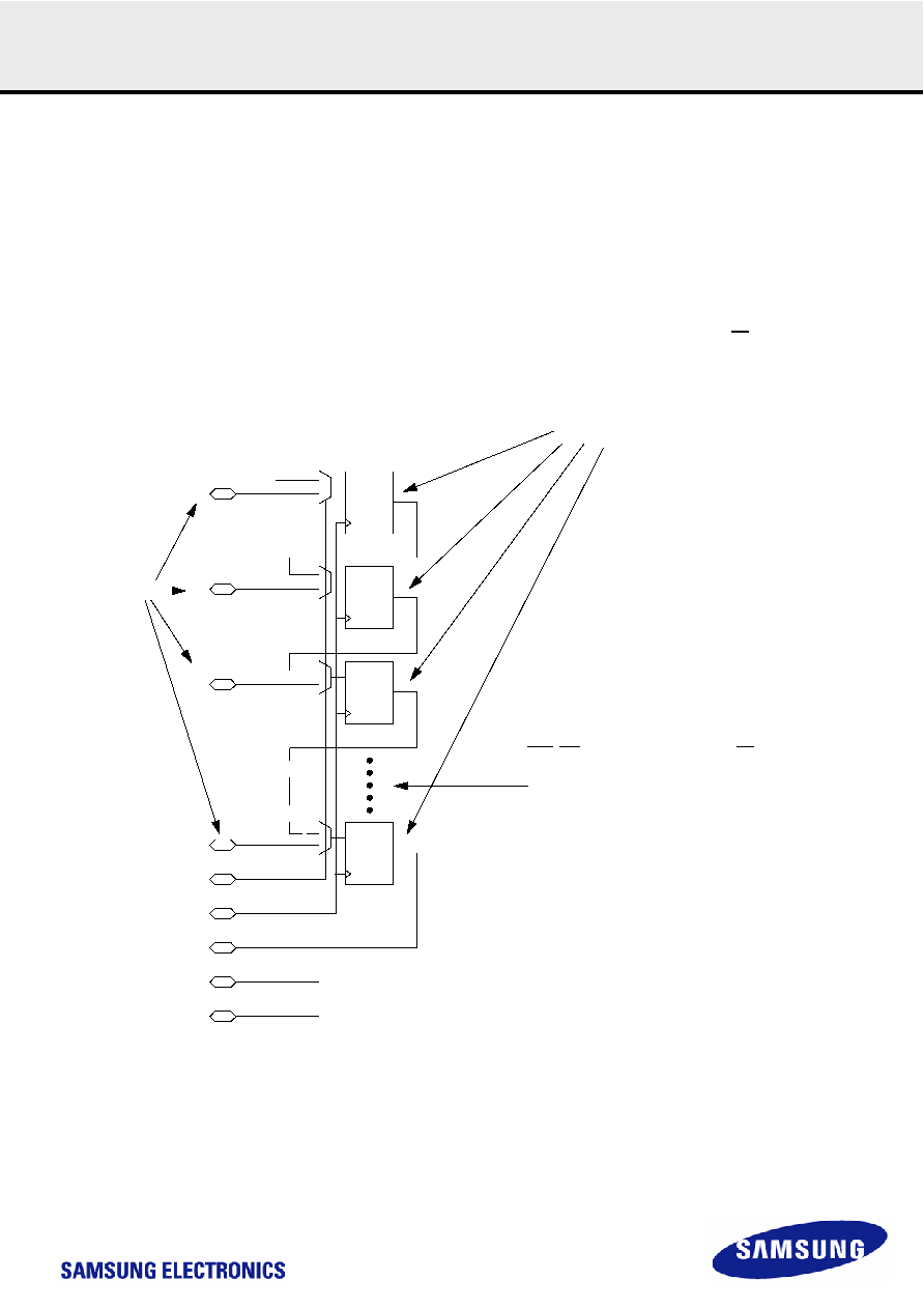
Figure 3. Internal Block Diagram (Reference Only)
Pins under test
CK
D
DQ
DM0
Tie to Iogic 0
CK
D
DQ
DQS
CK
D
DQ
DQ4
CK
D
DQ
RDQS0
RES (SSH,Scan Shift)
CS# (SCK, Scan Clock)
MF (SOE#, Output Enable)
RFU at V-4 (SEN, Scan Enable)
WDQS0 (SOUT,Scan Out)
Puts device into scan mode and re-maps pins to scan functionality
Dedicated Scan Flops
(1per signal under test)
The following lists the rest of the signals on the scan chain:
DQ[3:0], DQ[31:6], RDQS[3:1], WDQS[3:1], DM[3:1], RFU,
CAS, WE, CKE, BA[2:0], A[11:0], CK, CK and ZQ
Two RFU’s(J-2 and J-3 on 136-ball package) will be on the
scan chain and will read as a logic "0"
The following lists signals not on the scan chain:
NC, VDD, VSS, VDDQ, VSSQ, VREF
In case ZQ pin is connected to the external resistor, it will
be read as logic "0". However, if the ZQ pin is open, it will
be read as floating. Accordingly, ZQ pin should be driven
by any signal.
相關(guān)PDF資料 |
PDF描述 |
|---|---|
| K4M64163PK-BE900 | 4M X 16 SYNCHRONOUS DRAM, 7 ns, PBGA54 |
| K507 | 2 ELEMENT, 2000 uH, GENERAL PURPOSE INDUCTOR |
| K001 | 2 ELEMENT, 2000 uH, GENERAL PURPOSE INDUCTOR |
| K004 | 2 ELEMENT, 500 uH, GENERAL PURPOSE INDUCTOR |
| K5A22NAU | KEYPAD SWITCH, SPST, MOMENTARY, 0.1A, 50VDC, 2 N, SURFACE MOUNT-STRAIGHT |
相關(guān)代理商/技術(shù)參數(shù) |
參數(shù)描述 |
|---|---|
| K4J52324QC | 制造商:SAMSUNG 制造商全稱:Samsung semiconductor 功能描述:512Mbit GDDR3 SDRAM |
| K4J52324QC-AC20000 | 制造商:Samsung Semiconductor 功能描述:GDDR3 SDRAM X32 BOC - Trays |
| K4J52324QC-BC14 | 制造商:SAMSUNG 制造商全稱:Samsung semiconductor 功能描述:512Mbit GDDR3 SDRAM |
| K4J52324QC-BC14000 | 制造商:Samsung Semiconductor 功能描述:GDDR3 SDRAM X32 BOC LEAD PART 10W - Trays |
| K4J52324QC-BC16 | 制造商:SAMSUNG 制造商全稱:Samsung semiconductor 功能描述:512Mbit GDDR3 SDRAM |
發(fā)布緊急采購,3分鐘左右您將得到回復(fù)。