- 您現(xiàn)在的位置:買賣IC網(wǎng) > PDF目錄296260 > K4J52324KI-HC1A0 512M X 1 DDR DRAM, 0.2 ns, PBGA136 PDF資料下載
參數(shù)資料
| 型號(hào): | K4J52324KI-HC1A0 |
| 元件分類: | DRAM |
| 英文描述: | 512M X 1 DDR DRAM, 0.2 ns, PBGA136 |
| 封裝: | HALOGEN FREE AND ROHS COMPLIANT, FBGA-136 |
| 文件頁數(shù): | 56/61頁 |
| 文件大小: | 1364K |
| 代理商: | K4J52324KI-HC1A0 |
第1頁第2頁第3頁第4頁第5頁第6頁第7頁第8頁第9頁第10頁第11頁第12頁第13頁第14頁第15頁第16頁第17頁第18頁第19頁第20頁第21頁第22頁第23頁第24頁第25頁第26頁第27頁第28頁第29頁第30頁第31頁第32頁第33頁第34頁第35頁第36頁第37頁第38頁第39頁第40頁第41頁第42頁第43頁第44頁第45頁第46頁第47頁第48頁第49頁第50頁第51頁第52頁第53頁第54頁第55頁當(dāng)前第56頁第57頁第58頁第59頁第60頁第61頁
- 6 -
K4J52324KI
datasheet
GDDR3 SGRAM
Rev. 1.2
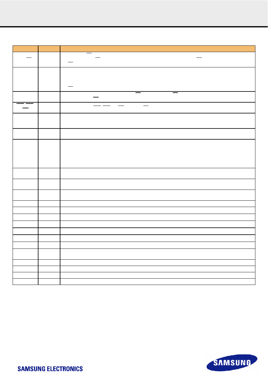
5. INPUT/OUTPUT FUNCTIONAL DESCRIPTION
Symbol
Type
Function
CK, CK
Input
Clock : CK and CK are differential clock inputs. CMD, ADD inputs are sampled on the crossing of the positive edge of CK
and negative edge of CK. Output (read) data is referenced to the crossings of CK and CK (both directions of crossing). CK
and CK should be maintained stable except self-refresh mode.
CKE
Input
Clock Enable : CKE HIGH activates, and CKE Low deactivates, internal clock signals and device input buffers and output
drivers. Taking CKE Low provides Precharge Power-Down and Self Refresh operation (all banks idle), or Active Power-
Down (row Active in any bank). CKE is synchronous for power down entry and exit, and for self refresh entry. CKE is asyn-
chronous for self refresh exit. CKE must be maintained high throughout read and write accesses. Input buffers, excluding
CK, CK and CKE are disabled during power-down. Input buffers, excluding CKE, are disabled during self refresh.
CS
Input
Chip Select : All commands are masked when CS is registered HIGH. CS provides for external bank selection on systems
with multiple banks. CS is considered part of the command code.
RAS, CAS,
WE
Input
Command Inputs : RAS, CAS and WE (along with CS) define the command being entered.
DM0
~DM3
Input
Input Data Mask : DM is an input mask signal for write data. Input data is masked when DM is sampled HIGH coincident
with that input data during a Write access. DM is sampled on both edges of clock. Although DM pins are input only, the DM
loading matches the DQ and WDQS loading.
BA0 ~ BA2
Input
Bank Address Inputs : BA0, BA1 and BA2 define to which bank an Active, Read, Write or Precharge command is being
applied.
A0 ~ A11
Input
Address Inputs : Provided the row address for Active commands and the column address and Auto Precharge bit for
Read/Write commands to select one location out of the memory array in the respective bank. A8 is sampled during a Pre-
charge command to determine whether the Precharge applies to one bank (A8 LOW) or all banks (A8 HIGH). If only one
bank is to be precharged, the bank is selected by BA0, BA1,BA2. The address inputs also provide the op-code during
Mode Register Set commands.
Row addresses : RA0 ~ RA11, Column addresses : CA0 ~ CA7, CA9 . Column address CA8 is used for auto precharge.
DQ0
~ DQ31
Input/
Output
Data Input/ Output: Bi-directional data bus.
RDQS0
~ RDQS3
Output
READ Data Strobe: Output with read data. RDQS is edge-aligned with read data.
WDQS0
~ WDQS3
Input
WRITE Data Strobe: Input with write data. WDQS is center-aligned to the input data.
NC/RFU
No Connect: No internal electrical connection is present.
VDDQ
Supply
DQ Power Supply
VSSQ
Supply
DQ Ground
VDD
Supply
Power Supply
VSS
Supply
Ground
VDDA
Supply
DLL Power Supply
VSSA
Supply
DLL Ground
VREF
Supply
Reference voltage: 0.7*VDDQ ,
2 Pins : (H12) for Data input , (H1) for CMD and ADDRESS
MF
Input
Mirror Function for clamshell mounting of DRAMs. VDDQ CMOS input.
ZQ
Reference Resistor connection pin for On-die termination.
RES
Input
Reset pin: RESET pin is a VDDQ CMOS input
SEN
Input
Scan enable : Must tie to the ground in case not in use. VDDQ CMOS input.
相關(guān)PDF資料 |
PDF描述 |
|---|---|
| K4M64163PK-BE900 | 4M X 16 SYNCHRONOUS DRAM, 7 ns, PBGA54 |
| K507 | 2 ELEMENT, 2000 uH, GENERAL PURPOSE INDUCTOR |
| K001 | 2 ELEMENT, 2000 uH, GENERAL PURPOSE INDUCTOR |
| K004 | 2 ELEMENT, 500 uH, GENERAL PURPOSE INDUCTOR |
| K5A22NAU | KEYPAD SWITCH, SPST, MOMENTARY, 0.1A, 50VDC, 2 N, SURFACE MOUNT-STRAIGHT |
相關(guān)代理商/技術(shù)參數(shù) |
參數(shù)描述 |
|---|---|
| K4J52324QC | 制造商:SAMSUNG 制造商全稱:Samsung semiconductor 功能描述:512Mbit GDDR3 SDRAM |
| K4J52324QC-AC20000 | 制造商:Samsung Semiconductor 功能描述:GDDR3 SDRAM X32 BOC - Trays |
| K4J52324QC-BC14 | 制造商:SAMSUNG 制造商全稱:Samsung semiconductor 功能描述:512Mbit GDDR3 SDRAM |
| K4J52324QC-BC14000 | 制造商:Samsung Semiconductor 功能描述:GDDR3 SDRAM X32 BOC LEAD PART 10W - Trays |
| K4J52324QC-BC16 | 制造商:SAMSUNG 制造商全稱:Samsung semiconductor 功能描述:512Mbit GDDR3 SDRAM |
發(fā)布緊急采購,3分鐘左右您將得到回復(fù)。