- 您現(xiàn)在的位置:買賣IC網(wǎng) > PDF目錄296260 > K4J52324KI-HC1A0 512M X 1 DDR DRAM, 0.2 ns, PBGA136 PDF資料下載
參數(shù)資料
| 型號(hào): | K4J52324KI-HC1A0 |
| 元件分類: | DRAM |
| 英文描述: | 512M X 1 DDR DRAM, 0.2 ns, PBGA136 |
| 封裝: | HALOGEN FREE AND ROHS COMPLIANT, FBGA-136 |
| 文件頁數(shù): | 52/61頁 |
| 文件大小: | 1364K |
| 代理商: | K4J52324KI-HC1A0 |
第1頁第2頁第3頁第4頁第5頁第6頁第7頁第8頁第9頁第10頁第11頁第12頁第13頁第14頁第15頁第16頁第17頁第18頁第19頁第20頁第21頁第22頁第23頁第24頁第25頁第26頁第27頁第28頁第29頁第30頁第31頁第32頁第33頁第34頁第35頁第36頁第37頁第38頁第39頁第40頁第41頁第42頁第43頁第44頁第45頁第46頁第47頁第48頁第49頁第50頁第51頁當(dāng)前第52頁第53頁第54頁第55頁第56頁第57頁第58頁第59頁第60頁第61頁
- 56 -
K4J52324KI
datasheet
GDDR3 SGRAM
Rev. 1.2
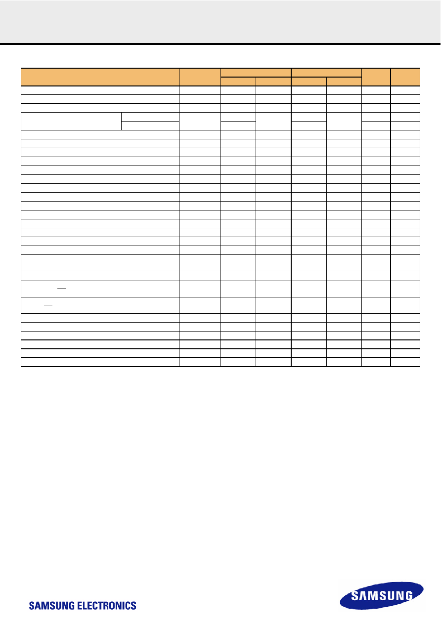
NOTE : 1. The WRITE latency can be set from 1 to 7 clocks. When the WRITE latency is set to 1 or 2 or 3 clocks, the input buffers are turned on during the
ACTIVE commands reducing the latency but added power. When the WRITE latency is set to 5 ~7 clocks which must be greater than 7ns, the
input buffers are turned on during the WRITE commands for lower power operation.
2. A low to high transition on the WDQS line is not allowed in the half clock prior to the write preamble.
3. The last rising edge of WDQS after the write postamble must be driven high by the controller. WDQS can not be pulled high by
the on-die termination alone.
4. tHZ and tLZ transitions occur in the same access time windows as valid data transitions. These parameters are not referenced to a specific
voltage level, but specify when the device output is no longer driving (HZ) or begins driving (LZ).
5. The cycle to cycle jitter over 1~6 cycle short term jitter
Parameter
Symbol
-HC12(800MHz)
-HC14(700MHz)
Unit
NOTE
Min
Max
Min
Max
DQS out access time from CK
tDQSCK
-0.23
+0.23
-0.26
+0.26
ns
CK high-level width
tCH
0.45
0.55
0.45
0.55
tCK
CK low-level width
tCL
0.45
0.55
0.45
0.55
tCK
CK cycle time
CL=11
tCK
1.25
3.3
-
3.3
ns
CL=10
1.4
ns
WRITE Latency
tWL
1,2,3,6,7
-
1,2,3,5,6,7
-
tCK
1
DQ and DM input hold time relative to DQS
tDH
0.16
-
0.18
-
ns
DQ and DM input setup time relative to DQS
tDS
0.16
-
0.18
-
ns
Active termination setup time
tATS
10
-
10
-
ns
Active termination hold time
tATH
10
-
10
-
ns
DQS input high pulse width
tDQSH
0.48
0.52
0.48
0.52
tCK
DQS input low pulse widthl
tDQSL
0.48
0.52
0.48
0.52
tCK
Data strobe edge to Dout edge
tDQSQ
-0.140
0.140
-0.160
0.160
ns
DQS read preamble
tRPRE
0.4
0.6
0.4
0.6
tCK
DQS read postamble
tRPST
0.4
0.6
0.4
0.6
tCK
Write command to first DQS latching transition
tDQSS
WL-0.2
WL+0.2
WL-0.2
WL+0.2
tCK
DQS write preamble
tWPRE
0.35
-
0.4
0.6
tCK
2
DQS write preamble setup time
tWPRES
0
-
0
-
ns
DQS write postamble
tWPST
0.4
0.6
0.4
0.6
tCK
3
Half strobe period
tHP
tCLmin or
tCHmin
-
tCLmin or
tCHmin
-tCK
Data output hold time from DQS
tQH
tHP-0.14
-
tHP-0.16
-ns
Data-out high-impedance window
from CK and CK
tHZ
-0.3
-
-0.3
-
ns
4
Data-out low-impedance window from
CK and CK
tLZ
-0.3
-
-0.3
-
ns
4
Address and control input hold time
tIH
0.3
-
0.35
-
ns
Address and control input setup time
tIS
0.3
-
0.35
-
ns
Address and control input pulse width
tIPW
0.9
-
1.0
-
ns
Jitter over 1~6 clock cycle error
tJ
-
0.03
-
0.03
tCK
5
Cycle to cycle duty cycle error
tDCERR
-
0.03
-
0.03
tCK
Rise and fall times of CK
tR, tF
-
0.2
-
0.2
tCK
相關(guān)PDF資料 |
PDF描述 |
|---|---|
| K4M64163PK-BE900 | 4M X 16 SYNCHRONOUS DRAM, 7 ns, PBGA54 |
| K507 | 2 ELEMENT, 2000 uH, GENERAL PURPOSE INDUCTOR |
| K001 | 2 ELEMENT, 2000 uH, GENERAL PURPOSE INDUCTOR |
| K004 | 2 ELEMENT, 500 uH, GENERAL PURPOSE INDUCTOR |
| K5A22NAU | KEYPAD SWITCH, SPST, MOMENTARY, 0.1A, 50VDC, 2 N, SURFACE MOUNT-STRAIGHT |
相關(guān)代理商/技術(shù)參數(shù) |
參數(shù)描述 |
|---|---|
| K4J52324QC | 制造商:SAMSUNG 制造商全稱:Samsung semiconductor 功能描述:512Mbit GDDR3 SDRAM |
| K4J52324QC-AC20000 | 制造商:Samsung Semiconductor 功能描述:GDDR3 SDRAM X32 BOC - Trays |
| K4J52324QC-BC14 | 制造商:SAMSUNG 制造商全稱:Samsung semiconductor 功能描述:512Mbit GDDR3 SDRAM |
| K4J52324QC-BC14000 | 制造商:Samsung Semiconductor 功能描述:GDDR3 SDRAM X32 BOC LEAD PART 10W - Trays |
| K4J52324QC-BC16 | 制造商:SAMSUNG 制造商全稱:Samsung semiconductor 功能描述:512Mbit GDDR3 SDRAM |
發(fā)布緊急采購,3分鐘左右您將得到回復(fù)。