- 您現在的位置:買賣IC網 > PDF目錄377798 > LXT386 (Intel Corp.) QUAD T1/E1/J1 Transceiver PDF資料下載
參數資料
| 型號: | LXT386 |
| 廠商: | Intel Corp. |
| 英文描述: | QUAD T1/E1/J1 Transceiver |
| 中文描述: | 四T1/E1/J1收發(fā)器 |
| 文件頁數: | 19/78頁 |
| 文件大?。?/td> | 500K |
| 代理商: | LXT386 |
第1頁第2頁第3頁第4頁第5頁第6頁第7頁第8頁第9頁第10頁第11頁第12頁第13頁第14頁第15頁第16頁第17頁第18頁當前第19頁第20頁第21頁第22頁第23頁第24頁第25頁第26頁第27頁第28頁第29頁第30頁第31頁第32頁第33頁第34頁第35頁第36頁第37頁第38頁第39頁第40頁第41頁第42頁第43頁第44頁第45頁第46頁第47頁第48頁第49頁第50頁第51頁第52頁第53頁第54頁第55頁第56頁第57頁第58頁第59頁第60頁第61頁第62頁第63頁第64頁第65頁第66頁第67頁第68頁第69頁第70頁第71頁第72頁第73頁第74頁第75頁第76頁第77頁第78頁
QUAD T1/E1/J1 Transceiver
—
LXT386
Datasheet
19
J11
98
CS/
JASEL
DI
DI
Chip Select/Jitter Attenuator Select.
Host Mode
This active Low input is used to access the serial/parallel interface. For
each read or write operation, CS must transition from High to Low, and
remain Low.
Hardware Mode
This input determines the Jitter Attenuator position in the data path:
H12
1
MOT/INTL/
CODEN
DI
DI
Motorola/Intel/Codec Enable Select.
Host Mode:
When Low, the host interface is configured for Motorola microcontrollers.
When High, the host interface is configured for Intel microcontrollers.
Hardware Mode:
This pin determines the line encode/decode selection when in un-
ipolar mode:
When Low, B8ZS/HDB3 encoders/decoders are enabled for T1/E1
respectively. When High, enables AMI encoder/decoder (transparent
mode).
G13
76
AT2
AO
JTAG Analog Output Test Port 2.
H13
77
AT1
AI
JTAG Analog Input Test Port 1.
G12
72
TRST
JTAG Controller Reset.
Input is used to reset the JTAG controller. TRST
is pulled up internally and may be left disconnected.
F11
71
TMS
DI
JTAG Test Mode Select.
Used to control the test logic state machine.
Sampled on rising edge of TCK. TMS is pulled up internally and may be
left disconnected.
F14
69
TCK
DI
JTAG Clock.
Clock input for JTAG. Connect to GND when not used.
F13
73
TDO
DO
JTAG Data Output.
Test Data Output for JTAG. Used for reading all
serial configuration and test data from internal test logic. Updated on
falling edge of TCK.
F12
70
TDI
DI
JTAG Data Input
. Test Data input for JTAG. Used for loading serial
instructions and data into internal test logic. Sampled on rising edge of
TCK. TDI is pulled up internally and may be left disconnected.
E14
83
OE
DI
Output Driver Enable.
If this pin is asserted Low all analog driver outputs
immediately enter a high impedance mode to support redundancy
applications without external mechanical relays. All other internal circuitry
stays active. In software mode, TTIP and TRING can be tristated on a
port-by-port basis by writing a
‘
1
’
to the OEx bit in the Output Enable
Register (OER).
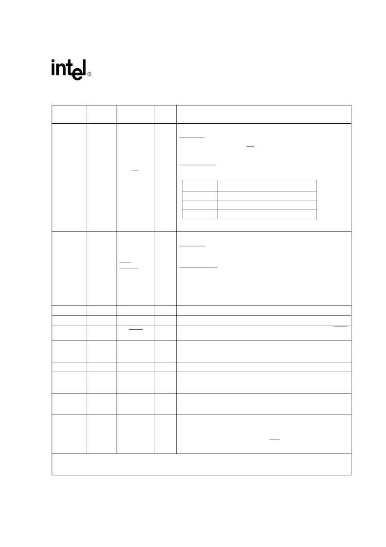
Table 1. Pin Assignments and Signal Descriptions
(Continued)
Ball #
PBGA
Pin #
LQFP
Symbol
I/O
1
Description
1. DI: Digital Input; DO: Digital Output; DI/O: Digital Bidirectional Port; AI: Analog Input; AO: Analog Output S: Power Supply;
N.C.: Not Connected.
2. N/C means
“
Not Connected
”
JASEL
JA Position
L
Transmit path
H
Receive path
Z
Disabled
相關PDF資料 |
PDF描述 |
|---|---|
| LXT400 | All Rate Extended Range Switched 56/DDS Transceiver |
| LXT441 | Switched 56/DDS Integrated DSU/CSU |
| LXT6155 | 155 Mbps SDH/SONET/ATM Transceiver |
| LXT6234 | E-Rate Multiplexer |
| LXT901 | 8QLYHUVDO (WKHUQHW 7UDQVFHLYHU |
相關代理商/技術參數 |
參數描述 |
|---|---|
| LXT386BE | 制造商:未知廠家 制造商全稱:未知廠家 功能描述:PCM TRANSCEIVER|QUAD|CEPT PCM-30/E-1|CMOS|BGA|160PIN|PLASTIC |
| LXT386LE | 制造商:LEVEL1 功能描述: |
| LXT388LE | 制造商:未知廠家 制造商全稱:未知廠家 功能描述:PCM TRANSCEIVER|DUAL|CEPT PCM-30/E-1|CMOS|QFP|100PIN|PLASTIC |
| LXT400 | 制造商:LVL1 制造商全稱:LVL1 功能描述:All Rate Extended Range Switched 56/DDS Transceiver |
| LXT400JE | 制造商:未知廠家 制造商全稱:未知廠家 功能描述:Transceiver Circuit For Telecommunications |
發(fā)布緊急采購,3分鐘左右您將得到回復。