- 您現(xiàn)在的位置:買賣IC網(wǎng) > PDF目錄377798 > LXT386 (Intel Corp.) QUAD T1/E1/J1 Transceiver PDF資料下載
參數(shù)資料
| 型號(hào): | LXT386 |
| 廠商: | Intel Corp. |
| 英文描述: | QUAD T1/E1/J1 Transceiver |
| 中文描述: | 四T1/E1/J1收發(fā)器 |
| 文件頁數(shù): | 20/78頁 |
| 文件大小: | 500K |
| 代理商: | LXT386 |
第1頁第2頁第3頁第4頁第5頁第6頁第7頁第8頁第9頁第10頁第11頁第12頁第13頁第14頁第15頁第16頁第17頁第18頁第19頁當(dāng)前第20頁第21頁第22頁第23頁第24頁第25頁第26頁第27頁第28頁第29頁第30頁第31頁第32頁第33頁第34頁第35頁第36頁第37頁第38頁第39頁第40頁第41頁第42頁第43頁第44頁第45頁第46頁第47頁第48頁第49頁第50頁第51頁第52頁第53頁第54頁第55頁第56頁第57頁第58頁第59頁第60頁第61頁第62頁第63頁第64頁第65頁第66頁第67頁第68頁第69頁第70頁第71頁第72頁第73頁第74頁第75頁第76頁第77頁第78頁
LXT386
—
QUAD T1/E1/J1 Transceiver
20
Datasheet
E13
84
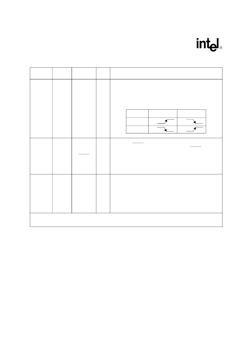
CLKE
DI
Clock Edge Select.
In clock recovery mode, setting CLKE High causes
RDATA or RPOS and RNEG to be valid on the falling edge of RCLK and
SDO to be valid on the rising edge of SCLK. Setting CLKE Low makes
RDATA or RPOS and RNEG to be valid on the rising edge of RCLK and
SDO to be valid on the falling edge of SCLK. In Data recovery Mode,
RDATA or RPOS/RNEG are active High output polarity when CLKE is
High and active low polarity when CLKE is Low.
N/C
2
100
RESET
DI
Reset Input.
(Added in Revision B1) In either hardware mode or software
mode, setting RESET low will begin to initialize the LXT386 and freeze the
device until set high. One microsecond after setting RESET high,
initialization will complete and the LXT386 will be ready for normal
operation. For Revision B1 only, the device requires a pull up resistor to
VCC at this pin between 1 and 10 kohms in value. It is not necessary to
retain the pull up resistor for any other revision. Please refer to the section
on Reset Operation for more information. The BGA package does not
have this pin feature.
A6, A9
B: 1, 2, 3, 6,
9, 12, 13, 14
C6, C9
D: 1, 2, 3, 6,
9, 12, 13, 14
G4, G11
H4, H11
5, 7, 10,
11, 65, 66,
74
GND
S
Power Supply Ground.
Connect all pins to power supply ground.
Table 1. Pin Assignments and Signal Descriptions
(Continued)
Ball #
PBGA
Pin #
LQFP
Symbol
I/O
1
Description
1. DI: Digital Input; DO: Digital Output; DI/O: Digital Bidirectional Port; AI: Analog Input; AO: Analog Output S: Power Supply;
N.C.: Not Connected.
2. N/C means
“
Not Connected
”
CLKE RPOS/RNEG SDO
Low
High
SCLK
SCLK
RCLK
RCLK
相關(guān)PDF資料 |
PDF描述 |
|---|---|
| LXT400 | All Rate Extended Range Switched 56/DDS Transceiver |
| LXT441 | Switched 56/DDS Integrated DSU/CSU |
| LXT6155 | 155 Mbps SDH/SONET/ATM Transceiver |
| LXT6234 | E-Rate Multiplexer |
| LXT901 | 8QLYHUVDO (WKHUQHW 7UDQVFHLYHU |
相關(guān)代理商/技術(shù)參數(shù) |
參數(shù)描述 |
|---|---|
| LXT386BE | 制造商:未知廠家 制造商全稱:未知廠家 功能描述:PCM TRANSCEIVER|QUAD|CEPT PCM-30/E-1|CMOS|BGA|160PIN|PLASTIC |
| LXT386LE | 制造商:LEVEL1 功能描述: |
| LXT388LE | 制造商:未知廠家 制造商全稱:未知廠家 功能描述:PCM TRANSCEIVER|DUAL|CEPT PCM-30/E-1|CMOS|QFP|100PIN|PLASTIC |
| LXT400 | 制造商:LVL1 制造商全稱:LVL1 功能描述:All Rate Extended Range Switched 56/DDS Transceiver |
| LXT400JE | 制造商:未知廠家 制造商全稱:未知廠家 功能描述:Transceiver Circuit For Telecommunications |
發(fā)布緊急采購,3分鐘左右您將得到回復(fù)。