- 您現(xiàn)在的位置:買賣IC網(wǎng) > PDF目錄377798 > LXT386 (Intel Corp.) QUAD T1/E1/J1 Transceiver PDF資料下載
參數(shù)資料
| 型號(hào): | LXT386 |
| 廠商: | Intel Corp. |
| 英文描述: | QUAD T1/E1/J1 Transceiver |
| 中文描述: | 四T1/E1/J1收發(fā)器 |
| 文件頁數(shù): | 37/78頁 |
| 文件大小: | 500K |
| 代理商: | LXT386 |
第1頁第2頁第3頁第4頁第5頁第6頁第7頁第8頁第9頁第10頁第11頁第12頁第13頁第14頁第15頁第16頁第17頁第18頁第19頁第20頁第21頁第22頁第23頁第24頁第25頁第26頁第27頁第28頁第29頁第30頁第31頁第32頁第33頁第34頁第35頁第36頁當(dāng)前第37頁第38頁第39頁第40頁第41頁第42頁第43頁第44頁第45頁第46頁第47頁第48頁第49頁第50頁第51頁第52頁第53頁第54頁第55頁第56頁第57頁第58頁第59頁第60頁第61頁第62頁第63頁第64頁第65頁第66頁第67頁第68頁第69頁第70頁第71頁第72頁第73頁第74頁第75頁第76頁第77頁第78頁
QUAD T1/E1/J1 Transceiver
—
LXT386
Datasheet
37
occurs, the INT pin is asserted Low. The output stage of the INT pin consists only of a pull-down
device; an external pull-up resistor of approximately 10k ohm is required to support wired-OR
operation.
3.13.2
Interrupt Clear
When an interrupt occurs, the interrupt service routine (ISR) should read the
interrupt status
registers
(08H, 09H and 15H) to identify the interrupt source. Reading the Interrupt Status register
clears the
“
sticky
”
bit set by the interrupt. Automatically clearing the register prepares it for the
next interrupt.
The ISR should then read the corresponding
status monitor register
to obtain the current status of
the device. Note that there are three status monitor registers: the LOS (04H), the DFM (05H) and
the AIS (013H). Reading either status monitors register will clear its corresponding interrupts on
the rising edge of the read or data strobe. When all pending interrupts are cleared, the INT pin goes
High.
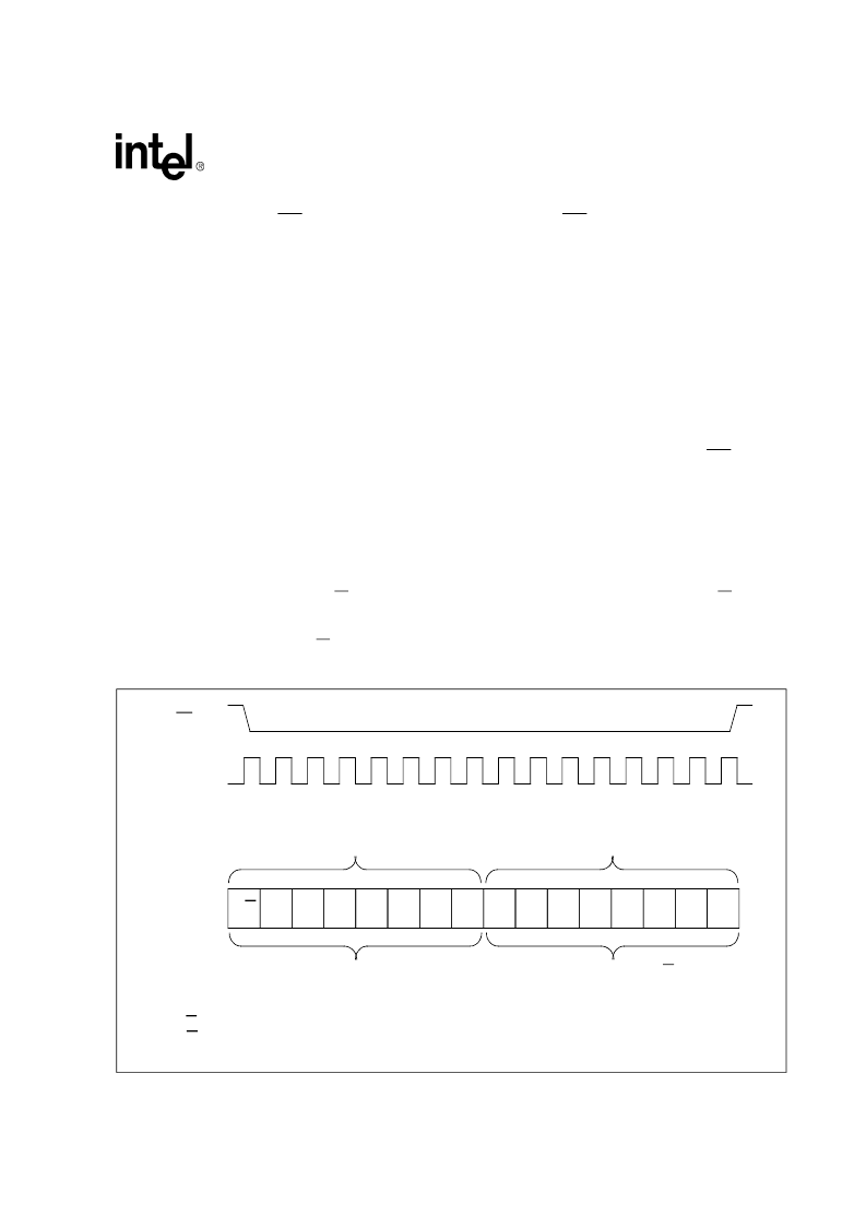
3.14
Serial Host Mode
The LXT386 operates in Serial Host Mode when the MODE pin is tied to VCC
÷
2.
Figure 14
shows
the SIO data structure. The registers are accessible through a 16 bit word: an 8bit Command/
Address byte (bits R/W and A1-A7) and a subsequent 8bit data byte (bits D0-7). Bit R/W
determines whether a read or a write operation occurs. Bits A5-0 in the Command/Address byte
address specific registers (the address decoder ignores bits A7-6). The data byte depends on both
the value of bit R/W and the address of the register as set in the Command/Address byte.
Figure 14. Serial Host Mode Timing
CS
SCLK
ADDRESS/COMMAND BYTE
INPUT DATA BYTE
R/W
A1
A2
A3
A4
A5
A6
X
A7
X
D0
D1
D2
D3
D4
D5
D6
D7
SDI
SDO - REMAINS HIGH Z
R/W
= 1: Read from the LXT386
R/W
= 0: Write to the LXT386
X
= Don
’
t care
SDO IS DRIVEN IF R/W = 1
相關(guān)PDF資料 |
PDF描述 |
|---|---|
| LXT400 | All Rate Extended Range Switched 56/DDS Transceiver |
| LXT441 | Switched 56/DDS Integrated DSU/CSU |
| LXT6155 | 155 Mbps SDH/SONET/ATM Transceiver |
| LXT6234 | E-Rate Multiplexer |
| LXT901 | 8QLYHUVDO (WKHUQHW 7UDQVFHLYHU |
相關(guān)代理商/技術(shù)參數(shù) |
參數(shù)描述 |
|---|---|
| LXT386BE | 制造商:未知廠家 制造商全稱:未知廠家 功能描述:PCM TRANSCEIVER|QUAD|CEPT PCM-30/E-1|CMOS|BGA|160PIN|PLASTIC |
| LXT386LE | 制造商:LEVEL1 功能描述: |
| LXT388LE | 制造商:未知廠家 制造商全稱:未知廠家 功能描述:PCM TRANSCEIVER|DUAL|CEPT PCM-30/E-1|CMOS|QFP|100PIN|PLASTIC |
| LXT400 | 制造商:LVL1 制造商全稱:LVL1 功能描述:All Rate Extended Range Switched 56/DDS Transceiver |
| LXT400JE | 制造商:未知廠家 制造商全稱:未知廠家 功能描述:Transceiver Circuit For Telecommunications |
發(fā)布緊急采購,3分鐘左右您將得到回復(fù)。