- 您現(xiàn)在的位置:買賣IC網(wǎng) > PDF目錄377496 > INTEL82801 (Intel Corp.) 82801AB (ICH0) I/O Controller Hub PDF資料下載
參數(shù)資料
| 型號(hào): | INTEL82801 |
| 廠商: | Intel Corp. |
| 英文描述: | 82801AB (ICH0) I/O Controller Hub |
| 中文描述: | 82801AB(ICH0)I / O控制器集線器 |
| 文件頁(yè)數(shù): | 119/414頁(yè) |
| 文件大小: | 2140K |
| 代理商: | INTEL82801 |
第1頁(yè)第2頁(yè)第3頁(yè)第4頁(yè)第5頁(yè)第6頁(yè)第7頁(yè)第8頁(yè)第9頁(yè)第10頁(yè)第11頁(yè)第12頁(yè)第13頁(yè)第14頁(yè)第15頁(yè)第16頁(yè)第17頁(yè)第18頁(yè)第19頁(yè)第20頁(yè)第21頁(yè)第22頁(yè)第23頁(yè)第24頁(yè)第25頁(yè)第26頁(yè)第27頁(yè)第28頁(yè)第29頁(yè)第30頁(yè)第31頁(yè)第32頁(yè)第33頁(yè)第34頁(yè)第35頁(yè)第36頁(yè)第37頁(yè)第38頁(yè)第39頁(yè)第40頁(yè)第41頁(yè)第42頁(yè)第43頁(yè)第44頁(yè)第45頁(yè)第46頁(yè)第47頁(yè)第48頁(yè)第49頁(yè)第50頁(yè)第51頁(yè)第52頁(yè)第53頁(yè)第54頁(yè)第55頁(yè)第56頁(yè)第57頁(yè)第58頁(yè)第59頁(yè)第60頁(yè)第61頁(yè)第62頁(yè)第63頁(yè)第64頁(yè)第65頁(yè)第66頁(yè)第67頁(yè)第68頁(yè)第69頁(yè)第70頁(yè)第71頁(yè)第72頁(yè)第73頁(yè)第74頁(yè)第75頁(yè)第76頁(yè)第77頁(yè)第78頁(yè)第79頁(yè)第80頁(yè)第81頁(yè)第82頁(yè)第83頁(yè)第84頁(yè)第85頁(yè)第86頁(yè)第87頁(yè)第88頁(yè)第89頁(yè)第90頁(yè)第91頁(yè)第92頁(yè)第93頁(yè)第94頁(yè)第95頁(yè)第96頁(yè)第97頁(yè)第98頁(yè)第99頁(yè)第100頁(yè)第101頁(yè)第102頁(yè)第103頁(yè)第104頁(yè)第105頁(yè)第106頁(yè)第107頁(yè)第108頁(yè)第109頁(yè)第110頁(yè)第111頁(yè)第112頁(yè)第113頁(yè)第114頁(yè)第115頁(yè)第116頁(yè)第117頁(yè)第118頁(yè)當(dāng)前第119頁(yè)第120頁(yè)第121頁(yè)第122頁(yè)第123頁(yè)第124頁(yè)第125頁(yè)第126頁(yè)第127頁(yè)第128頁(yè)第129頁(yè)第130頁(yè)第131頁(yè)第132頁(yè)第133頁(yè)第134頁(yè)第135頁(yè)第136頁(yè)第137頁(yè)第138頁(yè)第139頁(yè)第140頁(yè)第141頁(yè)第142頁(yè)第143頁(yè)第144頁(yè)第145頁(yè)第146頁(yè)第147頁(yè)第148頁(yè)第149頁(yè)第150頁(yè)第151頁(yè)第152頁(yè)第153頁(yè)第154頁(yè)第155頁(yè)第156頁(yè)第157頁(yè)第158頁(yè)第159頁(yè)第160頁(yè)第161頁(yè)第162頁(yè)第163頁(yè)第164頁(yè)第165頁(yè)第166頁(yè)第167頁(yè)第168頁(yè)第169頁(yè)第170頁(yè)第171頁(yè)第172頁(yè)第173頁(yè)第174頁(yè)第175頁(yè)第176頁(yè)第177頁(yè)第178頁(yè)第179頁(yè)第180頁(yè)第181頁(yè)第182頁(yè)第183頁(yè)第184頁(yè)第185頁(yè)第186頁(yè)第187頁(yè)第188頁(yè)第189頁(yè)第190頁(yè)第191頁(yè)第192頁(yè)第193頁(yè)第194頁(yè)第195頁(yè)第196頁(yè)第197頁(yè)第198頁(yè)第199頁(yè)第200頁(yè)第201頁(yè)第202頁(yè)第203頁(yè)第204頁(yè)第205頁(yè)第206頁(yè)第207頁(yè)第208頁(yè)第209頁(yè)第210頁(yè)第211頁(yè)第212頁(yè)第213頁(yè)第214頁(yè)第215頁(yè)第216頁(yè)第217頁(yè)第218頁(yè)第219頁(yè)第220頁(yè)第221頁(yè)第222頁(yè)第223頁(yè)第224頁(yè)第225頁(yè)第226頁(yè)第227頁(yè)第228頁(yè)第229頁(yè)第230頁(yè)第231頁(yè)第232頁(yè)第233頁(yè)第234頁(yè)第235頁(yè)第236頁(yè)第237頁(yè)第238頁(yè)第239頁(yè)第240頁(yè)第241頁(yè)第242頁(yè)第243頁(yè)第244頁(yè)第245頁(yè)第246頁(yè)第247頁(yè)第248頁(yè)第249頁(yè)第250頁(yè)第251頁(yè)第252頁(yè)第253頁(yè)第254頁(yè)第255頁(yè)第256頁(yè)第257頁(yè)第258頁(yè)第259頁(yè)第260頁(yè)第261頁(yè)第262頁(yè)第263頁(yè)第264頁(yè)第265頁(yè)第266頁(yè)第267頁(yè)第268頁(yè)第269頁(yè)第270頁(yè)第271頁(yè)第272頁(yè)第273頁(yè)第274頁(yè)第275頁(yè)第276頁(yè)第277頁(yè)第278頁(yè)第279頁(yè)第280頁(yè)第281頁(yè)第282頁(yè)第283頁(yè)第284頁(yè)第285頁(yè)第286頁(yè)第287頁(yè)第288頁(yè)第289頁(yè)第290頁(yè)第291頁(yè)第292頁(yè)第293頁(yè)第294頁(yè)第295頁(yè)第296頁(yè)第297頁(yè)第298頁(yè)第299頁(yè)第300頁(yè)第301頁(yè)第302頁(yè)第303頁(yè)第304頁(yè)第305頁(yè)第306頁(yè)第307頁(yè)第308頁(yè)第309頁(yè)第310頁(yè)第311頁(yè)第312頁(yè)第313頁(yè)第314頁(yè)第315頁(yè)第316頁(yè)第317頁(yè)第318頁(yè)第319頁(yè)第320頁(yè)第321頁(yè)第322頁(yè)第323頁(yè)第324頁(yè)第325頁(yè)第326頁(yè)第327頁(yè)第328頁(yè)第329頁(yè)第330頁(yè)第331頁(yè)第332頁(yè)第333頁(yè)第334頁(yè)第335頁(yè)第336頁(yè)第337頁(yè)第338頁(yè)第339頁(yè)第340頁(yè)第341頁(yè)第342頁(yè)第343頁(yè)第344頁(yè)第345頁(yè)第346頁(yè)第347頁(yè)第348頁(yè)第349頁(yè)第350頁(yè)第351頁(yè)第352頁(yè)第353頁(yè)第354頁(yè)第355頁(yè)第356頁(yè)第357頁(yè)第358頁(yè)第359頁(yè)第360頁(yè)第361頁(yè)第362頁(yè)第363頁(yè)第364頁(yè)第365頁(yè)第366頁(yè)第367頁(yè)第368頁(yè)第369頁(yè)第370頁(yè)第371頁(yè)第372頁(yè)第373頁(yè)第374頁(yè)第375頁(yè)第376頁(yè)第377頁(yè)第378頁(yè)第379頁(yè)第380頁(yè)第381頁(yè)第382頁(yè)第383頁(yè)第384頁(yè)第385頁(yè)第386頁(yè)第387頁(yè)第388頁(yè)第389頁(yè)第390頁(yè)第391頁(yè)第392頁(yè)第393頁(yè)第394頁(yè)第395頁(yè)第396頁(yè)第397頁(yè)第398頁(yè)第399頁(yè)第400頁(yè)第401頁(yè)第402頁(yè)第403頁(yè)第404頁(yè)第405頁(yè)第406頁(yè)第407頁(yè)第408頁(yè)第409頁(yè)第410頁(yè)第411頁(yè)第412頁(yè)第413頁(yè)第414頁(yè)
82801AA and 82801AB Datasheet
5-69
Functional Description
When the Bus Master IDE controller is reading data from the memory regions, bit 1 of the Base
Address is masked and byte enables are asserted for all read transfers. The controller reads to a
boundary of 64 bytes, regardless of byte count field of the PRD. Only the byte count value is
transferred to the drive however. When writing data, bit 1 of the Base Address is not masked and if
set, causes the lower Word byte enables to be deasserted for the first DWord transfer. The write to
PCI typically consists of a 32-byte cache line. If valid data ends prior to end of the cache line, the
byte enables are deasserted for invalid data.
The total sum of the byte counts in every PRD of the descriptor table must be equal to or greater
than the size of the disk transfer request. If greater than the disk transfer request, the driver must
terminate the bus master transaction (by setting bit 0 in the Bus Master IDE Command Register to
0) when the drive issues an interrupt to signal transfer completion.
5.14.2.2
Line Buffer
A single line buffer exists for the ICH Bus master IDE interface. This buffer is not shared with any
other function. The buffer is maintained in either the read state or the write state. Memory writes
are typically 4-DWord bursts and invalid DWords have C/BE[3:0]#=0Fh. The line buffer allows
burst data transfers to proceed at peak transfer rates.
The Bus Master IDE Active bit in Bus Master IDE Status register is reset automatically when the
controller has transferred all data associated with a Descriptor Table (as determined by EOT bit in
last PRD). The IDE Interrupt Status bit is set when the IDE device generates an interrupt. These
events may occur prior to line buffer emptying for memory writes. If either of these conditions
exist, all PCI Master non-memory read accesses to ICH are retried until all data in the line buffers
has been transferred to memory.
5.14.2.3
Bus Master IDE Timings
The timing modes used for Bus Master IDE transfers are identical to those for PIO transfers. The
DMA Timing Enable Only bits in IDE Timing register can be used to program fast timing mode for
DMA transactions only. This is useful for IDE devices whose DMA transfer timings are faster that
its PIO transfer timings. The IDE device DMA request signal is sampled on the same PCI clock
that DIOR# or DIOW# is deasserted. If inactive, the DMA Acknowledge signal is deasserted on
the next PCI clock and no more transfers take place until DMA request is asserted again.
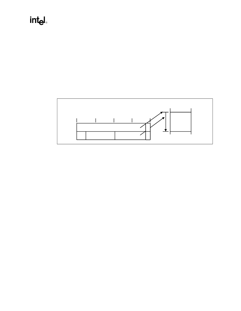
Figure 5-12. Physical Region Descriptor Table Entry
051910_3.drw
Byte 3
Byte 2
Byte 1
Byte 0
EOT
Reserved
Byte Count [15:1]
Memory Region Physical Base Address [31:1]
Memory
Region
Main Memory
0
0
相關(guān)PDF資料 |
PDF描述 |
|---|---|
| INTEL82802AB | Firmware Hub (FWH) |
| INTELDX2 | High-Performance 32-Bit Embedded Processor(高性能32位嵌入式處理器) |
| INTELDX4 | Embedded Write-Back Enhanced Processor(32位回復(fù)嵌入式增強(qiáng)型處理器) |
| IPS54511 | FULLY PROTECTED HIGH SIDE POWER MOSFET SWITCH |
| IPS5451 | FULLY PROTECTED HIGH SIDE POWER MOSFET SWITCH |
相關(guān)代理商/技術(shù)參數(shù) |
參數(shù)描述 |
|---|---|
| INTEL82802AB | 制造商:INTEL 制造商全稱:Intel Corporation 功能描述:Firmware Hub (FWH) |
| INTELLIGENT CHARGER + 4AA | 制造商:Energizer 功能描述:Bulk |
| INTELLI-INCH-LR-STARTER K | 制造商:ALL MOTION 功能描述:Intelli-Inch Stepper & Controller Starter Kit |
| INTELLIPANEL | 制造商:GJD 功能描述:EXTENSION LEAD 8GANG INTELLIPANEL 制造商:GJD 功能描述:EXTENSION LEAD, 8GANG, INTELLIPANEL |
| INTELLIPLUG | 制造商:GLOBAL COMMUNICATIONS 功能描述:ADAPTOR 3WAY INTELLIPLUG |
發(fā)布緊急采購(gòu),3分鐘左右您將得到回復(fù)。