- 您現(xiàn)在的位置:買賣IC網(wǎng) > PDF目錄369939 > P32P4911A (NXP SEMICONDUCTORS) PRML Read Channel with PR4, 8/9 ENDEC, FWR Servo PDF資料下載
參數(shù)資料
| 型號: | P32P4911A |
| 廠商: | NXP SEMICONDUCTORS |
| 元件分類: | 光電元器件 |
| 英文描述: | PRML Read Channel with PR4, 8/9 ENDEC, FWR Servo |
| 中文描述: | 1 CHANNEL READ CHANNEL, PQFP100 |
| 封裝: | 14 X 14 X 1.40 MM, PLASTIC, LQFP-100 |
| 文件頁數(shù): | 19/63頁 |
| 文件大小: | 257K |
| 代理商: | P32P4911A |
第1頁第2頁第3頁第4頁第5頁第6頁第7頁第8頁第9頁第10頁第11頁第12頁第13頁第14頁第15頁第16頁第17頁第18頁當(dāng)前第19頁第20頁第21頁第22頁第23頁第24頁第25頁第26頁第27頁第28頁第29頁第30頁第31頁第32頁第33頁第34頁第35頁第36頁第37頁第38頁第39頁第40頁第41頁第42頁第43頁第44頁第45頁第46頁第47頁第48頁第49頁第50頁第51頁第52頁第53頁第54頁第55頁第56頁第57頁第58頁第59頁第60頁第61頁第62頁第63頁

1996 Jul 25
19
Philips Semiconductors
Product specification
PRML Read Channel with PR4,
8/9 ENDEC, FWR Servo
P32P4911A
E
QUALIZATION
Q
UALITY
M
ONITOR
P
OINT
An equalization quality factor "Q" may be selected to be output on the ATO output pin by programming the ATOSEL bits
in the Power Down Register and should be used as a guide for selection of the appropriate value for km
2.
This signal is
derived by computing the absolute distance of the "real" and "canceled" zeros from the sampled data processor's system
ground which was established between the two zeros levels by the offset correction circuit. Then the asymmetry factor
(QASYM) is subtracted and the resulting signal is full wave rectified and low pass filtered using one of the four time
constants that may be programmed with the two QTC bits in the Control Operating Mode Register #2. The signal is then
buffered and differentially multiplexed to the ATO pin. The overall gain to the ATO pin is 4. The signal is referenced to
MAXREF/2.
The equalization quality factor can be held at the value present at sync byte detect by setting the FREZQ bit in the WP/LT
Register. The value will be held for approx. 10 ms and is NOT reset
.
The ATO output may also be externally filtered to
provide time constants that are appropriate for averaging over major portions of, or an entire sector. The capacitors on
externally added filters must be externally reset.
Time Base Generator Circuit Description
The time base generator (TBG) is a PLL based circuit, that provides a programmable reference frequency to the data
separator for constant density recording applications. This time base generator output frequency can be programmed
with a less than 1% accuracy via the M, N and DR Registers. The TBG output frequency, Fout, should be programmed
as close as possible to ((9/8) * NRZ Data Rate). The time base also supplies the timing reference for write
precompensation so that the precompensation tracks the reference time base period.
The time base generator requires an external passive loop filter to control its PLL locking characteristics. This filter is
fully-differential and balanced in order to reduce the effects of common mode noise.
In read, write and idle modes, the programmable time base generator is used to provide a stable reference frequency for
the data separator. In the write and idle modes, the Time Base Generator output, when selected by the Control Test
Mode Register, can be monitored at the TPB+ and TPB- test pins. In the read mode, the TBG output should not be
selected for output on the test pins so that the possibility of jitter in the data separator PLL is minimized.
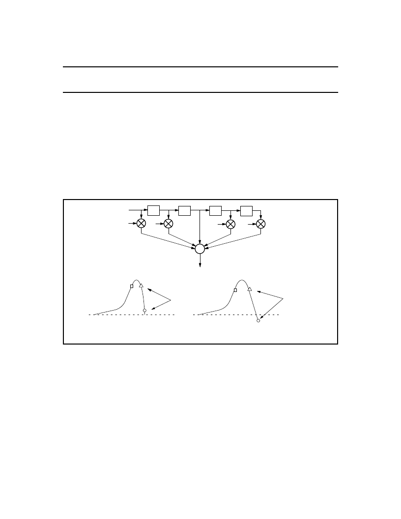
Figure 8: Block Diagram of 5-Tap Equalizer
y
n
= k
m2
x
n
+ k
m1
x
n-1
+ x
n-2
+ k
m1
x
n-3
+ k
m2
x
n-4
need more boost
decrease km
need less boost
increase km
+1
+1
+1
+1
0
0
0V
0V
D
D
D
D
x
n
x
n-1
x
n-2
x
n-3
x
n-4
k
m2
k
m1
k
m1
k
m2
y
n
k
m1
coefficient adapts to force ’0’ samples to 0V
SM00026
相關(guān)PDF資料 |
PDF描述 |
|---|---|
| P3500SA | SIDACtor Device |
| P3500S | SIDACtor Device |
| P3500SCMC | solid state crowbar devices |
| P3500SD | solid state crowbar devices |
| P3500SC | SIDACtor Device |
相關(guān)代理商/技術(shù)參數(shù) |
參數(shù)描述 |
|---|---|
| P32P4F-F | 制造商:TE Connectivity 功能描述: |
| P32RIGIDT | 制造商:Brady Corporation 功能描述:SIGN NO UNAUTHORISED PERSONS 250X200 |
| P32-S | 制造商:Linemaster Switch Corporation 功能描述:Premier |
| P32W2A2-100-7 | 功能描述:膠帶 Acrylic Foam Tape 1/32" x 1" x 7YD RoHS:否 制造商:3M Electronic Specialty 產(chǎn)品:Tapes 類型:Shielding 描述/功能:EMI/RFI Foil Shielding Tape 顏色: 材料:Copper Foil 寬度:1 in x 18 yds |
| P32W2A2-100-72 | 功能描述:膠帶 Acrylic Foam Tape 1/32" x 1" x 72YD RoHS:否 制造商:3M Electronic Specialty 產(chǎn)品:Tapes 類型:Shielding 描述/功能:EMI/RFI Foil Shielding Tape 顏色: 材料:Copper Foil 寬度:1 in x 18 yds |
發(fā)布緊急采購,3分鐘左右您將得到回復(fù)。