- 您現(xiàn)在的位置:買賣IC網(wǎng) > PDF目錄369939 > P32P4911A (NXP SEMICONDUCTORS) PRML Read Channel with PR4, 8/9 ENDEC, FWR Servo PDF資料下載
參數(shù)資料
| 型號(hào): | P32P4911A |
| 廠商: | NXP SEMICONDUCTORS |
| 元件分類: | 光電元器件 |
| 英文描述: | PRML Read Channel with PR4, 8/9 ENDEC, FWR Servo |
| 中文描述: | 1 CHANNEL READ CHANNEL, PQFP100 |
| 封裝: | 14 X 14 X 1.40 MM, PLASTIC, LQFP-100 |
| 文件頁(yè)數(shù): | 28/63頁(yè) |
| 文件大小: | 257K |
| 代理商: | P32P4911A |
第1頁(yè)第2頁(yè)第3頁(yè)第4頁(yè)第5頁(yè)第6頁(yè)第7頁(yè)第8頁(yè)第9頁(yè)第10頁(yè)第11頁(yè)第12頁(yè)第13頁(yè)第14頁(yè)第15頁(yè)第16頁(yè)第17頁(yè)第18頁(yè)第19頁(yè)第20頁(yè)第21頁(yè)第22頁(yè)第23頁(yè)第24頁(yè)第25頁(yè)第26頁(yè)第27頁(yè)當(dāng)前第28頁(yè)第29頁(yè)第30頁(yè)第31頁(yè)第32頁(yè)第33頁(yè)第34頁(yè)第35頁(yè)第36頁(yè)第37頁(yè)第38頁(yè)第39頁(yè)第40頁(yè)第41頁(yè)第42頁(yè)第43頁(yè)第44頁(yè)第45頁(yè)第46頁(yè)第47頁(yè)第48頁(yè)第49頁(yè)第50頁(yè)第51頁(yè)第52頁(yè)第53頁(yè)第54頁(yè)第55頁(yè)第56頁(yè)第57頁(yè)第58頁(yè)第59頁(yè)第60頁(yè)第61頁(yè)第62頁(yè)第63頁(yè)

1996 Jul 25
28
Philips Semiconductors
Product specification
PRML Read Channel with PR4,
8/9 ENDEC, FWR Servo
P32P4911A
a total of 6 byte times. Note that the semi-automatic mode can only be used to write single sync byte format and the
training pattern length is fixed at 5. This mode is useful if controller state machine space is extremely limited.
U
SER
D
ATA
The user data must be presented at the NRZ interface immediately following the last NRZ sync byte written. Finally, after
the last byte of user data has been clocked in, the WG/WG must remain active for a minimum of 16 NRZ bit times in
byte-wide mode to ensure the that the device is flushed of data (The delay is 21 NRZ bit times in nibble mode). WG/WG
can then go inactive. WD/WD stops toggling a maximum of 2 NRZ (RCLK) time periods after WG/WG goes inactive.
D
IRECT
W
RITE
M
ODE
#1
In this direct write mode, the NRZ data from the byte-wide interface bypasses the scrambler, the 8,9 encoder and the
precoder, but is precompensated before going to the write data flip-flop and then to the WD/WD output pins. The RCLK
output is changed from 9 VCO clock periods to 8 VCO clock periods with a 3/8 duty cycle. The purpose of routing the
signal to the precomp circuit is to generate a return to zero pulse every time a "1" occurs in the data so that the write data
flip-flop is toggled. WCLK is not required to latch the byte-wide NRZ data into the NRZ interface since the data is latched
by an internal version of RCLK, but the NRZ data must be valid no later than 12 ns after the rising edge of the RCLK
output pin. Direct write mode #1 is selected by setting the DW bit (bit 0) in the Control Operating Register. and is entered
when the WG/WG input is active. This mode is not valid when using the nibble NRZ interface. Note that Direct Write
Mode #2 will override Direct Write Mode #1.
D
IRECT
W
RITE
M
ODE
#2
In this direct write mode, the data presented at the DWI/DWI input pins directly toggles the write data flip-flop which drives
the WD/WD output pins. No WCLK is required in this mode, and the WD/WD output is not resynchronized. Direct write
mode #2 is selected by driving the DWR input Low and is entered when the WG/WG input is active. Note that the Direct
Write Mode #2 will override Direct Write Mode #1.
D
ATA
R
EAD
M
ODE
O
PERATION
Data read mode is initiated by setting the Read Gate (RG) input pin High. This action causes the data synchronizer to
begin acquisition of the clock from the incoming VCO sync pattern. To achieve this, the data synchronizer utilizes a fully
integrated fast acquisition PLL to accurately develop the sample clock. This PLL is normally locked to the time base
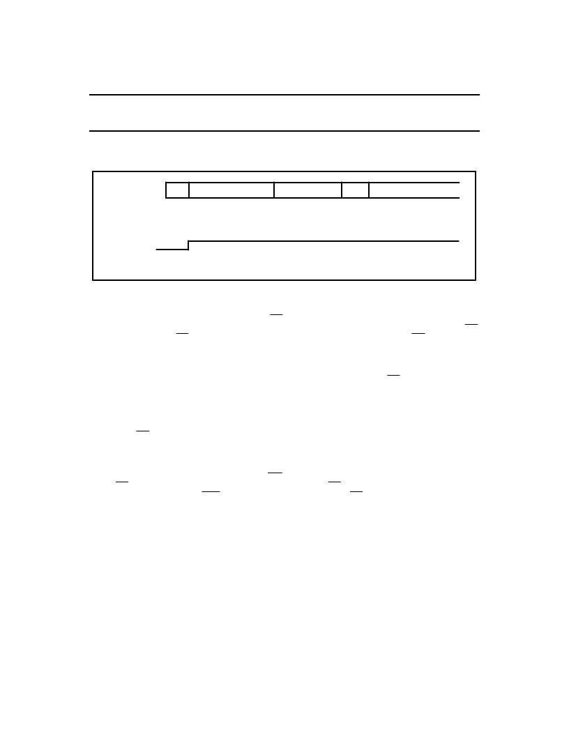
Figure 16: Hard Sector Semi-Auto Write Mode
GAP
8 BYTES MIN.
5 BYTES
1 BYTE
NRZ DATA (WRITTEN TO 4911A)
00H
FFH
FFH
USER DATA
WG
NRZ DATA (WRITTEN BY 4911A)
00H
93H
69H
USER DATA
VCO SYNC
FIELD
TRAINING
SEQUENCE
SYNC
BYTE
SCRAMBLED AND ENCODED
USER DATA
相關(guān)PDF資料 |
PDF描述 |
|---|---|
| P3500SA | SIDACtor Device |
| P3500S | SIDACtor Device |
| P3500SCMC | solid state crowbar devices |
| P3500SD | solid state crowbar devices |
| P3500SC | SIDACtor Device |
相關(guān)代理商/技術(shù)參數(shù) |
參數(shù)描述 |
|---|---|
| P32P4F-F | 制造商:TE Connectivity 功能描述: |
| P32RIGIDT | 制造商:Brady Corporation 功能描述:SIGN NO UNAUTHORISED PERSONS 250X200 |
| P32-S | 制造商:Linemaster Switch Corporation 功能描述:Premier |
| P32W2A2-100-7 | 功能描述:膠帶 Acrylic Foam Tape 1/32" x 1" x 7YD RoHS:否 制造商:3M Electronic Specialty 產(chǎn)品:Tapes 類型:Shielding 描述/功能:EMI/RFI Foil Shielding Tape 顏色: 材料:Copper Foil 寬度:1 in x 18 yds |
| P32W2A2-100-72 | 功能描述:膠帶 Acrylic Foam Tape 1/32" x 1" x 72YD RoHS:否 制造商:3M Electronic Specialty 產(chǎn)品:Tapes 類型:Shielding 描述/功能:EMI/RFI Foil Shielding Tape 顏色: 材料:Copper Foil 寬度:1 in x 18 yds |
發(fā)布緊急采購(gòu),3分鐘左右您將得到回復(fù)。