- 您現在的位置:買賣IC網 > PDF目錄374354 > KM416RD4C (SAMSUNG SEMICONDUCTOR CO. LTD.) Direct Rambus DRAM(Direct Rambus 動態(tài)RAM) PDF資料下載
參數資料
| 型號: | KM416RD4C |
| 廠商: | SAMSUNG SEMICONDUCTOR CO. LTD. |
| 英文描述: | Direct Rambus DRAM(Direct Rambus 動態(tài)RAM) |
| 中文描述: | 直接Rambus公司的DRAM(動態(tài)內存直接Rambus公司) |
| 文件頁數: | 21/59頁 |
| 文件大小: | 4654K |
| 代理商: | KM416RD4C |
第1頁第2頁第3頁第4頁第5頁第6頁第7頁第8頁第9頁第10頁第11頁第12頁第13頁第14頁第15頁第16頁第17頁第18頁第19頁第20頁當前第21頁第22頁第23頁第24頁第25頁第26頁第27頁第28頁第29頁第30頁第31頁第32頁第33頁第34頁第35頁第36頁第37頁第38頁第39頁第40頁第41頁第42頁第43頁第44頁第45頁第46頁第47頁第48頁第49頁第50頁第51頁第52頁第53頁第54頁第55頁第56頁第57頁第58頁第59頁
Page 22
KM416RD4C/KM418RD4C
Direct RDRAM
Revision 0.7 September 1998
TARGET
Write Transaction - Example
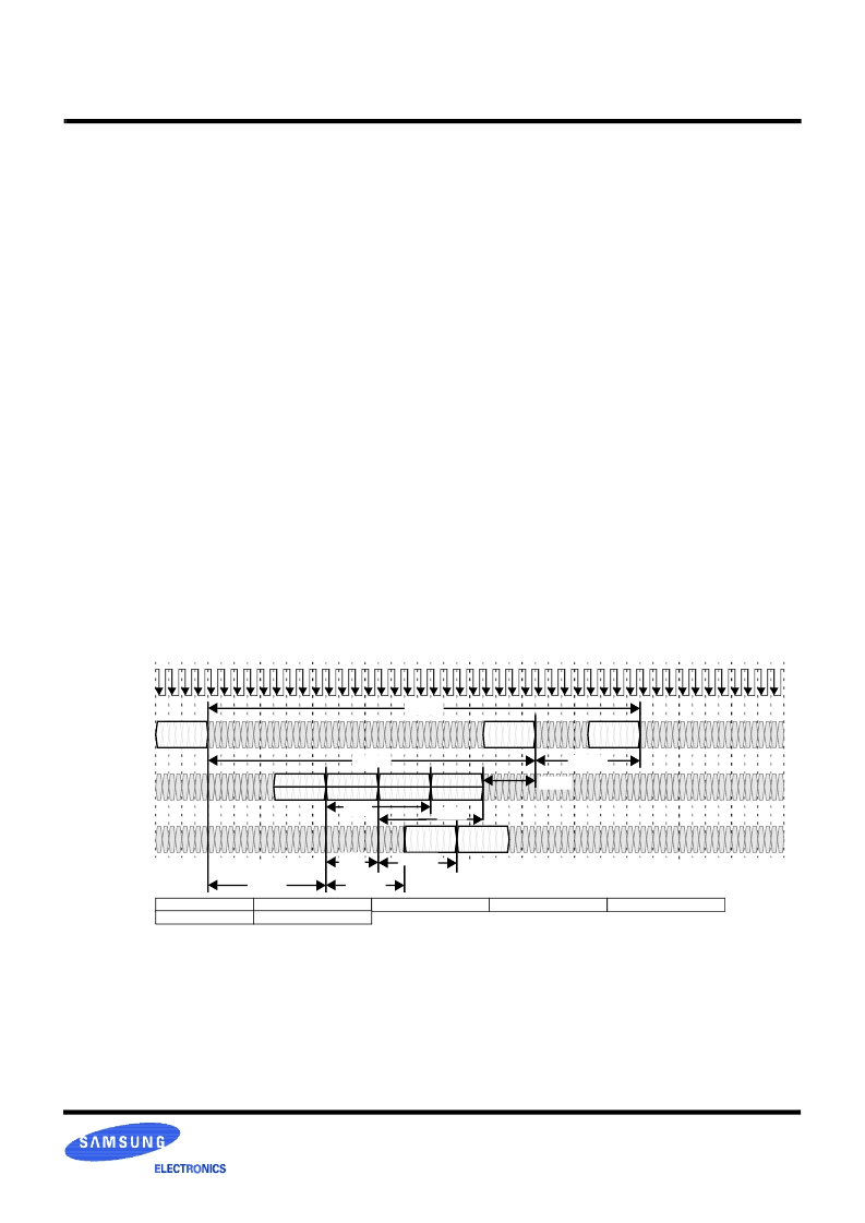
Figure Figure shows an example of a write transaction. It
begins by activating a bank with an ACT a0 command in an
ROWA packet. A time t
RCD
later a WR a1 command is
issued in a COLC packet. Note that the ACT command
includes the device, bank, and row address (abbreviated as
a0) while the WR command includes device, bank, and
column address (abbreviated as a1). A time t
CWD
after the
WR command the write data dualoct D(a1) is issued. Note
that the packets on the ROW and COL pins use the end of
the packet as a timing reference point, while the packets on
the DQA/DQB pins use the beginning of the packet as a
timing reference point.
A time t
CC
after the first COLC packet on the COL pins a
second COLC packet is issued. It contains a WR a2
command. The a2 address has the same device and bank
address as the a1 address (and a0 address), but a different
column address. A time t
CWD
after the second WR
command a second write data dualoct D(a2) is issued.
A time t
RTR
after each WR command an optional COLM
packet MSK (a1) is issued, and at the same time a COLC
packet is issued causing the write buffer to automatically
retire. See Figure Figure for more detail on the write/retire
mechanism. If a COLM packet is not used, all data bytes are
unconditionally written. If the COLC packet which causes
the write buffer to retire is delayed, then the COLM packet
(if used) must also be delayed.
Next, a PRER a3 command is issued in an ROWR packet on
the ROW pins. This causes the bank to precharge so that a
different row may be activated in a subsequent transaction or
so that an adjacent bank may be activated. The a3 address
includes the same device and bank address as the a0, a1, and
a2 addresses. The PRER command must occur a time t
RAS
or more after the original ACT command (the activation
operation in any DRAM is destructive, and the contents of
the selected row must be restored from the two associated
sense amps of the bank during the t
RAS
interval).
A PRER a3 command is issued in an ROWR packet on the
ROW pins. The PRER command must occur a time t
RTP
or
more after the last COLC which causes an automatic retire.
Finally, an ACT b0 command is issued in an ROWR packet
on the ROW pins. The second ACT command must occur a
time t
RC
or more after the first ACT command and a time t
RP
or more after the PRER command. This ensures that the
bank and its associated sense amps are precharged. This
example assumes that the second transaction has the same
device and bank address as the first transaction, but a
different row address. Transaction b may not be started until
transaction a has finished. However, transactions to other
banks or other devices may be issued during transaction a.
Figure 16 : Write Transaction Example
CTM/CFM
DQA8..0
DQB8..0
COL4
..COL0
ROW2
..ROW0
T
0
T
4
T
8
T
12
T
1
T
5
T
9
T
13
T
2
T
6
T
10
T
14
T
3
T
7
T
11
T
15
T
16
T
20
T
24
T
28
T
17
T
21
T
25
T
29
T
18
T
22
T
26
T
30
T
19
T
23
T
27
T
31
T
32
T
36
T
40
T
44
T
33
T
37
T
41
T
45
T
34
T
38
T
42
T
46
T
35
T
39
T
43
T
47
MSK (a2)
t
RTR
retire (a2)
MSK (a1)
retire (a1)
WR a1
PRER a3
WR a2
D (a2)
t
RCD
D (a1)
ACT b0
t
RC
t
RP
ACT a0
t
CWD
Transaction a: WR
Transaction b: xx
a0 = {Da,Ba,Ra}
b0 = {Da,Ba,Rb}
a1 = {Da,Ba,Ca1}
a2 = {Da,Ba,Ca2}
a3 = {Da,Ba}
t
CC
t
CWD
t
RTR
t
RAS
t
RTP
相關PDF資料 |
PDF描述 |
|---|---|
| KM416S1021CT-G7 | 512K x 16Bit x 2 Banks Synchronous DRAM with SSTL interface |
| KM416S1021CT-G8 | 512K x 16Bit x 2 Banks Synchronous DRAM with SSTL interface |
| KM416S1021CT-GS | 512K x 16Bit x 2 Banks Synchronous DRAM with SSTL interface |
| KM416S1120D | 512K x 16bit x 2 Banks Synchronous DRAM LVTTL |
| KM416S16230A | 4M x 16Bit x 4 Banks Synchronous DRAM(4M x 16位 x4組同步動態(tài)RAM) |
相關代理商/技術參數 |
參數描述 |
|---|---|
| KM416RD4D | 制造商:SAMSUNG 制造商全稱:Samsung semiconductor 功能描述:128/144Mbit RDRAM 256K x 16/18 bit x 2*16 Dependent Banks Direct RDRAMTM |
| KM416RD8AC | 制造商:SAMSUNG 制造商全稱:Samsung semiconductor 功能描述:128/144Mbit RDRAM 256K x 16/18 bit x 2*16 Dependent Banks Direct RDRAMTM |
| KM416RD8AC(D)-RK70 | 制造商:SAMSUNG 制造商全稱:Samsung semiconductor 功能描述:128/144Mbit RDRAM 256K x 16/18 bit x 2*16 Dependent Banks Direct RDRAMTM |
| KM416RD8AC(D)-RK80 | 制造商:SAMSUNG 制造商全稱:Samsung semiconductor 功能描述:128/144Mbit RDRAM 256K x 16/18 bit x 2*16 Dependent Banks Direct RDRAMTM |
| KM416RD8AC(DB)-RCG60 | 制造商:SAMSUNG 制造商全稱:Samsung semiconductor 功能描述:128/144Mbit RDRAM 256K x 16/18 bit x 2*16 Dependent Banks Direct RDRAMTM |
發(fā)布緊急采購,3分鐘左右您將得到回復。