- 您現(xiàn)在的位置:買賣IC網(wǎng) > PDF目錄374354 > KM416RD4C (SAMSUNG SEMICONDUCTOR CO. LTD.) Direct Rambus DRAM(Direct Rambus 動(dòng)態(tài)RAM) PDF資料下載
參數(shù)資料
| 型號(hào): | KM416RD4C |
| 廠商: | SAMSUNG SEMICONDUCTOR CO. LTD. |
| 英文描述: | Direct Rambus DRAM(Direct Rambus 動(dòng)態(tài)RAM) |
| 中文描述: | 直接Rambus公司的DRAM(動(dòng)態(tài)內(nèi)存直接Rambus公司) |
| 文件頁(yè)數(shù): | 38/59頁(yè) |
| 文件大小: | 4654K |
| 代理商: | KM416RD4C |
第1頁(yè)第2頁(yè)第3頁(yè)第4頁(yè)第5頁(yè)第6頁(yè)第7頁(yè)第8頁(yè)第9頁(yè)第10頁(yè)第11頁(yè)第12頁(yè)第13頁(yè)第14頁(yè)第15頁(yè)第16頁(yè)第17頁(yè)第18頁(yè)第19頁(yè)第20頁(yè)第21頁(yè)第22頁(yè)第23頁(yè)第24頁(yè)第25頁(yè)第26頁(yè)第27頁(yè)第28頁(yè)第29頁(yè)第30頁(yè)第31頁(yè)第32頁(yè)第33頁(yè)第34頁(yè)第35頁(yè)第36頁(yè)第37頁(yè)當(dāng)前第38頁(yè)第39頁(yè)第40頁(yè)第41頁(yè)第42頁(yè)第43頁(yè)第44頁(yè)第45頁(yè)第46頁(yè)第47頁(yè)第48頁(yè)第49頁(yè)第50頁(yè)第51頁(yè)第52頁(yè)第53頁(yè)第54頁(yè)第55頁(yè)第56頁(yè)第57頁(yè)第58頁(yè)第59頁(yè)
Page 39
KM416RD4C/KM418RD4C
Direct RDRAM
Revision 0.2 September 1998
TARGET
Power State Management
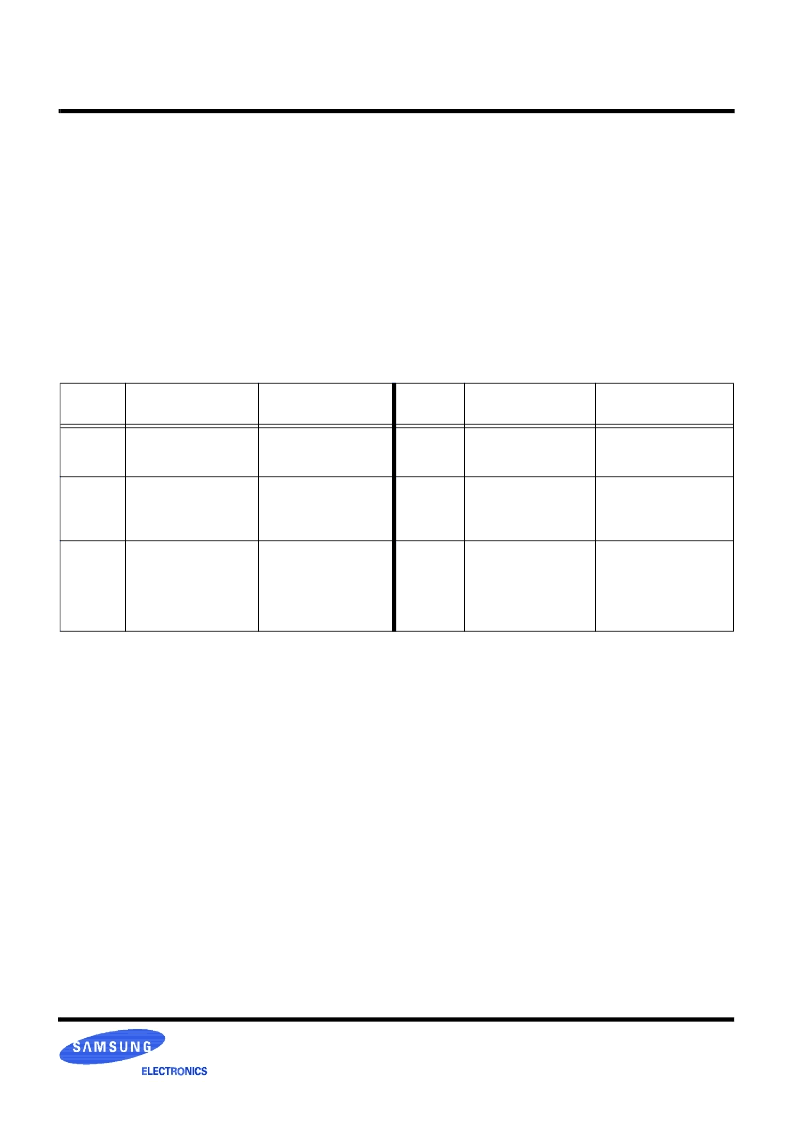
Table Table summarizes the power states available to a
Direct RDRAM. In general, the lowest power states have the
longest operational latencies. For example, the relative
power levels of PDN state and STBY state have a ratio of
about 1:110, and the relative access latencies to get read data
have a ratio of about 250:1.
PDN state is the lowest power state available. The informa-
tion in the RDRAM core is usually maintained with self-
refresh; an internal timer automatically refreshes all rows of
all banks. PDN has a relatively long exit latency because the
TCLK/RCLK block must resynchronize itself to the external
clock signal.
NAP state is another low-power state in which either self-
refresh or REFA-refresh are used to maintain the core. See
“Refresh” on page 43 for a description of the two refresh
mechanisms. NAP has a shorter exit latency than PDN
because the TCLK/RCLK block maintains its synchroniza-
tion state relative to the external clock signal at the time of
NAP entry. This imposes a limit (t
NLIMIT
) on how long an
RDRAM may remain in NAP state before briefly returning
to STBY or ATTN to update this synchronization state.
Figure Figure summarizes the transition conditions needed
for moving between the various power states. Note that NAP
and PDN have been divided into two substates (NAP-A/
NAP-S and PDN-A/PDN-S) to account for the fact that a
NAP or PDN exit may be made to either ATTN or STBY
states.
At initialization, the SETR/CLRR Reset sequence will put
the RDRAM into PDN-S state. The PDN exit sequence
involves an optional PDEV specification and bits on the
CMD and SIO
IN
pins.
Once the RDRAM is in STBY, it will move to the ATTN/
ATTNR/ATTNW states when it receives a non-broadcast
ROWA packet or non-broadcast ROWR packet with the
ATTN command. The RDRAM returns to STBY from these
three states when it receives a RLX command. Alternatively,
it may enter NAP or PDN state from ATTN or STBY states
with a NAPR or PDNR command in an ROWR packet. The
PDN or NAP exit sequence involves an optional PDEV spec-
ification and bits on the CMD and SIO0 pins. The RDRAM
returns to the ATTN or STBY state it was originally in when
it first entered NAP or PDN.
An RDRAM may only remain in NAP state for a time
t
NLIMIT
. It must periodically return to ATTN or STBY.
The NAPRC command causes a napdown operation if the
RDRAM’s NCBIT is set. The NCBIT is not directly visible.
It is undefined on reset. It is set by a NAP or NAPRC
command to the RDRAM, and it is cleared by an ACT
command to the RDRAM. It permits a controller to manage a
set of RDRAMs in a mixture of power states.
STBY state is the normal idle state of the RDRAM. In this
state all banks and sense amps have usually been left
precharged and ROWA and ROWR packets on the ROW
pins are being monitored. When a non-broadcast ROWA
packet or non-broadcast ROWR packet (with the ATTN
command) packet addressed to the RDRAM is seen, the
RDRAM enters ATTN state (see the right side of
Figure Figure). This requires a time t
SA
during which the
RDRAM activates the specified row of the specified bank. A
time TFRMt
CYCLE
after the ROW packet, the RDRAM will
be
Table 17 : Power State Summary
Power
State
Description
Blocks consuming power
Power
State
Description
Blocks consuming power
PDN
Powerdown state.
Self-refresh
NAP
Nap state. Similar to PDN
except lower wake-up
latency.
Self-refresh or
REFA-refresh
TCLK/RCLK-Nap
STBY
Standby state.
Ready for ROW
packets.
REFA-refresh
TCLK/RCLK
ROW demux receiver
ATTN
Attention state.
Ready for ROW and COL
packets.
REFA-refresh
TCLK/RCLK
ROW demux receiver
COL demux receiver
ATTNR
Attention read state.
Ready for ROW and COL
packets.
Sending Q (read data)
packets.
REFA-refresh
TCLK/RCLK
ROW demux receiver
COL demux receiver
DQ mux transmitter
Core power
ATTNW
Attention write state.
Ready for ROW and COL
packets.
Ready for D (write data)
packets.
REFA-refresh
TCLK/RCLK
ROW demux receiver
COL demux receiver
DQ demux receiver
Core power
相關(guān)PDF資料 |
PDF描述 |
|---|---|
| KM416S1021CT-G7 | 512K x 16Bit x 2 Banks Synchronous DRAM with SSTL interface |
| KM416S1021CT-G8 | 512K x 16Bit x 2 Banks Synchronous DRAM with SSTL interface |
| KM416S1021CT-GS | 512K x 16Bit x 2 Banks Synchronous DRAM with SSTL interface |
| KM416S1120D | 512K x 16bit x 2 Banks Synchronous DRAM LVTTL |
| KM416S16230A | 4M x 16Bit x 4 Banks Synchronous DRAM(4M x 16位 x4組同步動(dòng)態(tài)RAM) |
相關(guān)代理商/技術(shù)參數(shù) |
參數(shù)描述 |
|---|---|
| KM416RD4D | 制造商:SAMSUNG 制造商全稱:Samsung semiconductor 功能描述:128/144Mbit RDRAM 256K x 16/18 bit x 2*16 Dependent Banks Direct RDRAMTM |
| KM416RD8AC | 制造商:SAMSUNG 制造商全稱:Samsung semiconductor 功能描述:128/144Mbit RDRAM 256K x 16/18 bit x 2*16 Dependent Banks Direct RDRAMTM |
| KM416RD8AC(D)-RK70 | 制造商:SAMSUNG 制造商全稱:Samsung semiconductor 功能描述:128/144Mbit RDRAM 256K x 16/18 bit x 2*16 Dependent Banks Direct RDRAMTM |
| KM416RD8AC(D)-RK80 | 制造商:SAMSUNG 制造商全稱:Samsung semiconductor 功能描述:128/144Mbit RDRAM 256K x 16/18 bit x 2*16 Dependent Banks Direct RDRAMTM |
| KM416RD8AC(DB)-RCG60 | 制造商:SAMSUNG 制造商全稱:Samsung semiconductor 功能描述:128/144Mbit RDRAM 256K x 16/18 bit x 2*16 Dependent Banks Direct RDRAMTM |
發(fā)布緊急采購(gòu),3分鐘左右您將得到回復(fù)。