- 您現(xiàn)在的位置:買賣IC網(wǎng) > PDF目錄374354 > KM416RD4C (SAMSUNG SEMICONDUCTOR CO. LTD.) Direct Rambus DRAM(Direct Rambus 動態(tài)RAM) PDF資料下載
參數(shù)資料
| 型號: | KM416RD4C |
| 廠商: | SAMSUNG SEMICONDUCTOR CO. LTD. |
| 英文描述: | Direct Rambus DRAM(Direct Rambus 動態(tài)RAM) |
| 中文描述: | 直接Rambus公司的DRAM(動態(tài)內存直接Rambus公司) |
| 文件頁數(shù): | 54/59頁 |
| 文件大小: | 4654K |
| 代理商: | KM416RD4C |
第1頁第2頁第3頁第4頁第5頁第6頁第7頁第8頁第9頁第10頁第11頁第12頁第13頁第14頁第15頁第16頁第17頁第18頁第19頁第20頁第21頁第22頁第23頁第24頁第25頁第26頁第27頁第28頁第29頁第30頁第31頁第32頁第33頁第34頁第35頁第36頁第37頁第38頁第39頁第40頁第41頁第42頁第43頁第44頁第45頁第46頁第47頁第48頁第49頁第50頁第51頁第52頁第53頁當前第54頁第55頁第56頁第57頁第58頁第59頁
Page 55
KM416RD4C/KM418RD4C
Direct RDRAM
Revision 0.2 September 1998
TARGET
Timing Parameters
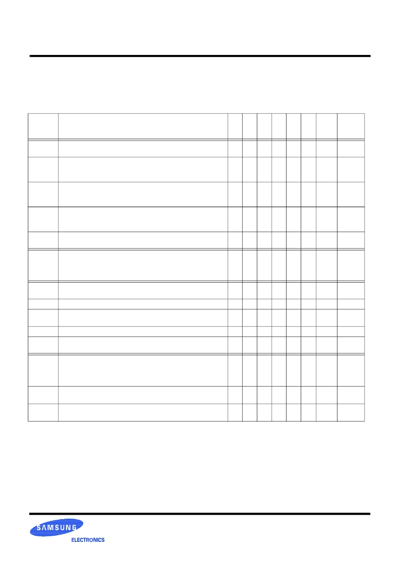
Table Timing Parameter Summary
Parameter
Description
Min
-40
-800
Min
-45
-800
Min
-50
-800
Min
-45
-600
Min
-53
-600
Max Units
Figure(s)
t
RC
Row Cycle time of RDRAM banks -the interval between ROWA packets
with ACT commands to the same bank.
28
28
34
22
28
-
t
CYCLE
Figure 15
Figure 16
t
RAS
RAS-asserted time of RDRAM bank - the interval between ROWA packet
with ACT command and next ROWR packet with PRER
a
command to the
same bank.
20
20
24
16
20
-
b
t
CYCLE
Figure 15
Figure 16
t
RP
Row Precharge time of RDRAM banks - the interval between ROWR packet
with PRER
a
command and next ROWA packet with ACT command to the
same bank.
8
8
10
6
8
-
t
CYCLE
Figure 15
Figure 16
t
PP
Precharge-to-precharge time of RDRAM device - the interval between suc-
cessive ROWR packets with PRER
a
commands to any banks of the same
device.
8
8
8
8
8
-
t
CYCLE
Figure 12
t
RR
RAS-to-RAS time of RDRAM device - the interval between successive
ROWA packets with ACT commands to any banks of the same device.
8
8
8
8
8
-
t
CYCLE
Figure 13
t
RCD
RAS-to-CAS Delay - the interval from ROWA packet with ACT command
to COLC packet with RD or WR command). Note - the RAS-to-CAS delay
seen by the RDRAM core (t
RCD-C
) is equal to t
RCD-C
= 1 + t
RCD
because of
differences in the row and column paths through the RDRAM interface.
7
9
11
5
7
-
t
CYCLE
Figure 15
Figure 16
t
CAC
CAS Access delay - the interval from RD command to Q read data. The
equation for t
CAC
is given in the TPARM register in Figure 39.
8
8
8
7
8
12
t
CYCLE
Figure 4
Figure 39
t
CWD
CAS Write Delay (interval from WR command to D write data.
6
6
6
6
6
6
t
CYCLE
Figure 4
t
CC
CAS-to-CAS time of RDRAM bank - the interval between successive COLC
commands).
4
4
4
4
4
-
t
CYCLE
Figure 15
Figure 16
t
PACKET
Length of ROWA, ROWR, COLC, COLM or COLX packet.
4
4
4
4
4
4
t
CYCLE
Figure 3
t
RTR
Interval from COLC packet with WR command to COLC packet which
causes retire, and to COLM packet with bytemask.
8
8
8
8
8
-
t
CYCLE
Figure 17
t
OFFP
The interval (offset) from COLC packet with RDA command, or from COLC
packet with retire command (after WRA automatic precharge), or from
COLX packet with PREX command to the equivalent ROWR packet with
PRER.The equation for t
OFFP
is given in the TPARM register in Figure 39.
4
4
4
4
4
4
t
CYCLE
Figure 14
Figure 39
t
RDP
Interval from last COLC packet with RD command to ROWR packet with
PRER.
4
4
4
4
4
-
t
CYCLE
Figure 15
t
RTP
Interval from last COLC packet with automatic retire command to ROWR
packet with PRER.
4
4
4
4
4
-
t
CYCLE
Figure 16
a.Or equivalent PREC or PREX command. See Figure 14.
b.See t
RAS,MAX
value in “Timing Conditions” on page 45.
相關PDF資料 |
PDF描述 |
|---|---|
| KM416S1021CT-G7 | 512K x 16Bit x 2 Banks Synchronous DRAM with SSTL interface |
| KM416S1021CT-G8 | 512K x 16Bit x 2 Banks Synchronous DRAM with SSTL interface |
| KM416S1021CT-GS | 512K x 16Bit x 2 Banks Synchronous DRAM with SSTL interface |
| KM416S1120D | 512K x 16bit x 2 Banks Synchronous DRAM LVTTL |
| KM416S16230A | 4M x 16Bit x 4 Banks Synchronous DRAM(4M x 16位 x4組同步動態(tài)RAM) |
相關代理商/技術參數(shù) |
參數(shù)描述 |
|---|---|
| KM416RD4D | 制造商:SAMSUNG 制造商全稱:Samsung semiconductor 功能描述:128/144Mbit RDRAM 256K x 16/18 bit x 2*16 Dependent Banks Direct RDRAMTM |
| KM416RD8AC | 制造商:SAMSUNG 制造商全稱:Samsung semiconductor 功能描述:128/144Mbit RDRAM 256K x 16/18 bit x 2*16 Dependent Banks Direct RDRAMTM |
| KM416RD8AC(D)-RK70 | 制造商:SAMSUNG 制造商全稱:Samsung semiconductor 功能描述:128/144Mbit RDRAM 256K x 16/18 bit x 2*16 Dependent Banks Direct RDRAMTM |
| KM416RD8AC(D)-RK80 | 制造商:SAMSUNG 制造商全稱:Samsung semiconductor 功能描述:128/144Mbit RDRAM 256K x 16/18 bit x 2*16 Dependent Banks Direct RDRAMTM |
| KM416RD8AC(DB)-RCG60 | 制造商:SAMSUNG 制造商全稱:Samsung semiconductor 功能描述:128/144Mbit RDRAM 256K x 16/18 bit x 2*16 Dependent Banks Direct RDRAMTM |
發(fā)布緊急采購,3分鐘左右您將得到回復。