- 您現(xiàn)在的位置:買賣IC網(wǎng) > PDF目錄361671 > V4ECFUM ColdFire CF4e Core User's Manual PDF資料下載
參數(shù)資料
| 型號(hào): | V4ECFUM |
| 英文描述: | ColdFire CF4e Core User's Manual |
| 中文描述: | 核心的ColdFire CF4e用戶手冊(cè) |
| 文件頁(yè)數(shù): | 216/372頁(yè) |
| 文件大?。?/td> | 4286K |
| 代理商: | V4ECFUM |
第1頁(yè)第2頁(yè)第3頁(yè)第4頁(yè)第5頁(yè)第6頁(yè)第7頁(yè)第8頁(yè)第9頁(yè)第10頁(yè)第11頁(yè)第12頁(yè)第13頁(yè)第14頁(yè)第15頁(yè)第16頁(yè)第17頁(yè)第18頁(yè)第19頁(yè)第20頁(yè)第21頁(yè)第22頁(yè)第23頁(yè)第24頁(yè)第25頁(yè)第26頁(yè)第27頁(yè)第28頁(yè)第29頁(yè)第30頁(yè)第31頁(yè)第32頁(yè)第33頁(yè)第34頁(yè)第35頁(yè)第36頁(yè)第37頁(yè)第38頁(yè)第39頁(yè)第40頁(yè)第41頁(yè)第42頁(yè)第43頁(yè)第44頁(yè)第45頁(yè)第46頁(yè)第47頁(yè)第48頁(yè)第49頁(yè)第50頁(yè)第51頁(yè)第52頁(yè)第53頁(yè)第54頁(yè)第55頁(yè)第56頁(yè)第57頁(yè)第58頁(yè)第59頁(yè)第60頁(yè)第61頁(yè)第62頁(yè)第63頁(yè)第64頁(yè)第65頁(yè)第66頁(yè)第67頁(yè)第68頁(yè)第69頁(yè)第70頁(yè)第71頁(yè)第72頁(yè)第73頁(yè)第74頁(yè)第75頁(yè)第76頁(yè)第77頁(yè)第78頁(yè)第79頁(yè)第80頁(yè)第81頁(yè)第82頁(yè)第83頁(yè)第84頁(yè)第85頁(yè)第86頁(yè)第87頁(yè)第88頁(yè)第89頁(yè)第90頁(yè)第91頁(yè)第92頁(yè)第93頁(yè)第94頁(yè)第95頁(yè)第96頁(yè)第97頁(yè)第98頁(yè)第99頁(yè)第100頁(yè)第101頁(yè)第102頁(yè)第103頁(yè)第104頁(yè)第105頁(yè)第106頁(yè)第107頁(yè)第108頁(yè)第109頁(yè)第110頁(yè)第111頁(yè)第112頁(yè)第113頁(yè)第114頁(yè)第115頁(yè)第116頁(yè)第117頁(yè)第118頁(yè)第119頁(yè)第120頁(yè)第121頁(yè)第122頁(yè)第123頁(yè)第124頁(yè)第125頁(yè)第126頁(yè)第127頁(yè)第128頁(yè)第129頁(yè)第130頁(yè)第131頁(yè)第132頁(yè)第133頁(yè)第134頁(yè)第135頁(yè)第136頁(yè)第137頁(yè)第138頁(yè)第139頁(yè)第140頁(yè)第141頁(yè)第142頁(yè)第143頁(yè)第144頁(yè)第145頁(yè)第146頁(yè)第147頁(yè)第148頁(yè)第149頁(yè)第150頁(yè)第151頁(yè)第152頁(yè)第153頁(yè)第154頁(yè)第155頁(yè)第156頁(yè)第157頁(yè)第158頁(yè)第159頁(yè)第160頁(yè)第161頁(yè)第162頁(yè)第163頁(yè)第164頁(yè)第165頁(yè)第166頁(yè)第167頁(yè)第168頁(yè)第169頁(yè)第170頁(yè)第171頁(yè)第172頁(yè)第173頁(yè)第174頁(yè)第175頁(yè)第176頁(yè)第177頁(yè)第178頁(yè)第179頁(yè)第180頁(yè)第181頁(yè)第182頁(yè)第183頁(yè)第184頁(yè)第185頁(yè)第186頁(yè)第187頁(yè)第188頁(yè)第189頁(yè)第190頁(yè)第191頁(yè)第192頁(yè)第193頁(yè)第194頁(yè)第195頁(yè)第196頁(yè)第197頁(yè)第198頁(yè)第199頁(yè)第200頁(yè)第201頁(yè)第202頁(yè)第203頁(yè)第204頁(yè)第205頁(yè)第206頁(yè)第207頁(yè)第208頁(yè)第209頁(yè)第210頁(yè)第211頁(yè)第212頁(yè)第213頁(yè)第214頁(yè)第215頁(yè)當(dāng)前第216頁(yè)第217頁(yè)第218頁(yè)第219頁(yè)第220頁(yè)第221頁(yè)第222頁(yè)第223頁(yè)第224頁(yè)第225頁(yè)第226頁(yè)第227頁(yè)第228頁(yè)第229頁(yè)第230頁(yè)第231頁(yè)第232頁(yè)第233頁(yè)第234頁(yè)第235頁(yè)第236頁(yè)第237頁(yè)第238頁(yè)第239頁(yè)第240頁(yè)第241頁(yè)第242頁(yè)第243頁(yè)第244頁(yè)第245頁(yè)第246頁(yè)第247頁(yè)第248頁(yè)第249頁(yè)第250頁(yè)第251頁(yè)第252頁(yè)第253頁(yè)第254頁(yè)第255頁(yè)第256頁(yè)第257頁(yè)第258頁(yè)第259頁(yè)第260頁(yè)第261頁(yè)第262頁(yè)第263頁(yè)第264頁(yè)第265頁(yè)第266頁(yè)第267頁(yè)第268頁(yè)第269頁(yè)第270頁(yè)第271頁(yè)第272頁(yè)第273頁(yè)第274頁(yè)第275頁(yè)第276頁(yè)第277頁(yè)第278頁(yè)第279頁(yè)第280頁(yè)第281頁(yè)第282頁(yè)第283頁(yè)第284頁(yè)第285頁(yè)第286頁(yè)第287頁(yè)第288頁(yè)第289頁(yè)第290頁(yè)第291頁(yè)第292頁(yè)第293頁(yè)第294頁(yè)第295頁(yè)第296頁(yè)第297頁(yè)第298頁(yè)第299頁(yè)第300頁(yè)第301頁(yè)第302頁(yè)第303頁(yè)第304頁(yè)第305頁(yè)第306頁(yè)第307頁(yè)第308頁(yè)第309頁(yè)第310頁(yè)第311頁(yè)第312頁(yè)第313頁(yè)第314頁(yè)第315頁(yè)第316頁(yè)第317頁(yè)第318頁(yè)第319頁(yè)第320頁(yè)第321頁(yè)第322頁(yè)第323頁(yè)第324頁(yè)第325頁(yè)第326頁(yè)第327頁(yè)第328頁(yè)第329頁(yè)第330頁(yè)第331頁(yè)第332頁(yè)第333頁(yè)第334頁(yè)第335頁(yè)第336頁(yè)第337頁(yè)第338頁(yè)第339頁(yè)第340頁(yè)第341頁(yè)第342頁(yè)第343頁(yè)第344頁(yè)第345頁(yè)第346頁(yè)第347頁(yè)第348頁(yè)第349頁(yè)第350頁(yè)第351頁(yè)第352頁(yè)第353頁(yè)第354頁(yè)第355頁(yè)第356頁(yè)第357頁(yè)第358頁(yè)第359頁(yè)第360頁(yè)第361頁(yè)第362頁(yè)第363頁(yè)第364頁(yè)第365頁(yè)第366頁(yè)第367頁(yè)第368頁(yè)第369頁(yè)第370頁(yè)第371頁(yè)第372頁(yè)
9-2
ColdFire CF4E Core User’s Manual
For More Information On This Product,
Go to: www.freescale.com
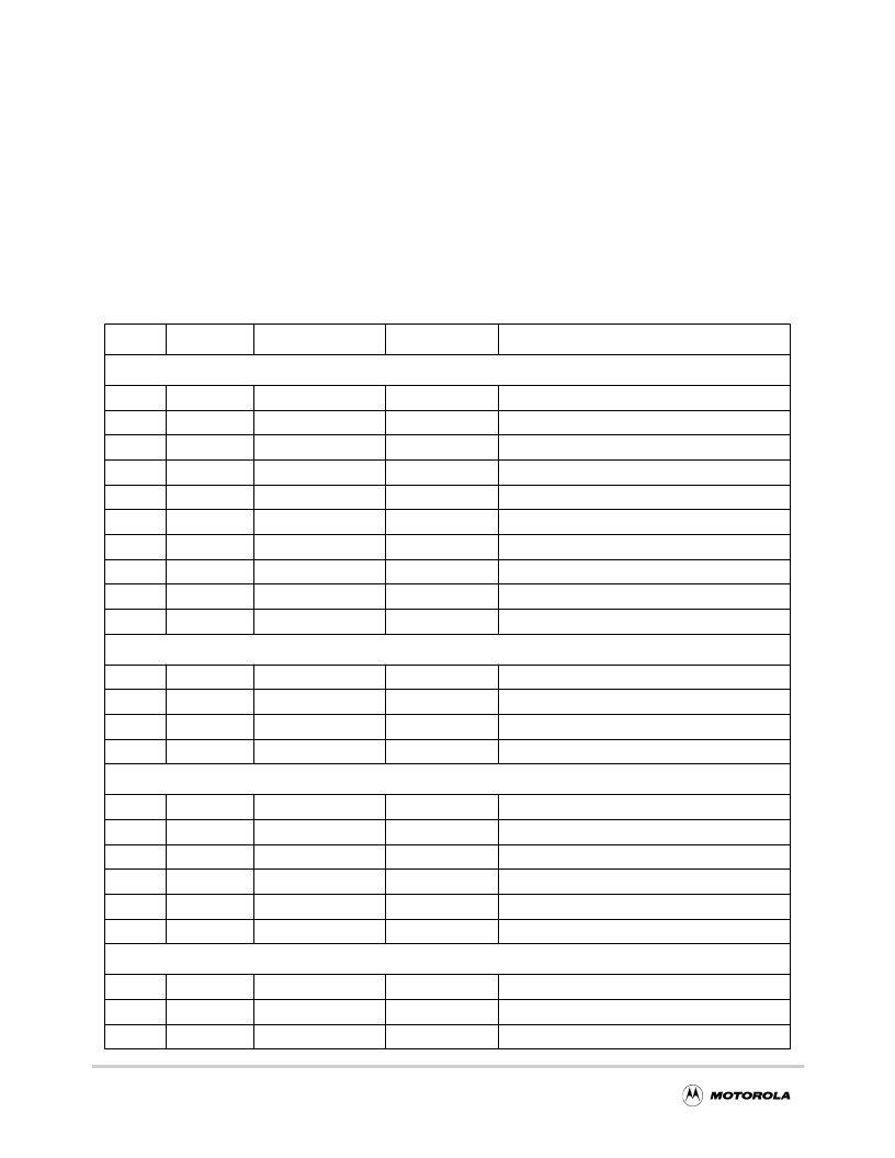
CF4e Pin Characteristics
9.2 CF4e Pin Characteristics
Table 9-1 provides CF4e core pin characteristics. Most M-Bus and debug input signals are
driven directly into input capture registers in the CF4e core. K-Bus memories are specified
as synchronous; CF4e core outputs are next-state values registered in the memory device.
NOTE:
The letter ‘b’ at the end of a name indicates an active-low
signal.
Table 9-1. CF4e Pin Characteristics
No.
Type
Name
Bus Width
1
Description
M-Bus Outputs
1
Output
maddr
[31:0]
M-Bus address
2
Output
mtt
[1:0]
M-Bus transfer type
3
Output
mtm
[2:0]
M-Bus transfer modifier
4
Output
mrwb
—
M-Bus read/write
5
Output
msiz
[1:0]
M-Bus transfer size
6
Output
mwdata
[31:0]
M-Bus write data
7
Output
mwdataoe
—
M-Bus output enable
8
Output
mapb
—
M-Bus address phase
9
Output
mdpb
—
M-Bus data phase
10
Output
mlockb
—
M-Bus locked access
Debug Outputs
11
Output
bdmforceackb
—
BDM force M-Bus acknowledge
12
Output
cpustopb
—
Processor is stopped
13
Output
cpuhaltb
—
Processor is halted
14
Output
pstclk
—
PST/DDATA clock
Test Outputs
15
Output
so
[42:0]
Core parallel scan outputs
16
Output
tbso
[7:0]
Test boundary scan outputs
17
Output
bistdone
—
BIST done indicator
18
Output
bistdata
3:0]
BIST bitmap data
19
Output
bistfail
—
BIST memory failure indicator
20
Output
bisthold
—
BIST holding indicator
Outputs to K-Bus Memories
21
Output
nsientb
—
Next-state I-cache tag enable
22
Output
nsiwrttb
—
Next-state I-cache tag write
23
Output
nsiwlvt
[3:0]
Next-state I-cache tag write level
F
Freescale Semiconductor, Inc.
n
.
相關(guān)PDF資料 |
PDF描述 |
|---|---|
| V4F-1J-01V | HYBRIDKARTENLESER |
| V4F-1J-01V565246 | READER CARD |
| V4NS | MICROSWITCH PLUNGER |
| V4NST7 | MICROSWITCH PLUNGER |
| V4NST8 | MICROSWITCH PLUNGER |
相關(guān)代理商/技術(shù)參數(shù) |
參數(shù)描述 |
|---|---|
| V4F-10P | 功能描述:3M PELTOR CLEAR POLYCARB 制造商:3m 系列:* 零件狀態(tài):在售 標(biāo)準(zhǔn)包裝:1 |
| V4FFS12V40A | 制造商:TDK 功能描述:Vega universal input SMPSU,12V 450W |
| V4FFS24V15A | 制造商:TDK 功能描述:Vega universal input SMPSU,24V 450W |
| V4FFS5V60A,12V12A,12V12A,24V6 | 制造商:TDK 功能描述:Vega univ input SMPSU,5/2x12/24V 450W |
| V4FFS5Z18F12C3F12B3F | 制造商:TDK 功能描述:Vega universal input SMPSU,5/2x12V 450W |
發(fā)布緊急采購(gòu),3分鐘左右您將得到回復(fù)。