- 您現(xiàn)在的位置:買賣IC網(wǎng) > PDF目錄371179 > T8110 Version History PDF資料下載
參數(shù)資料
| 型號: | T8110 |
| 英文描述: | Version History |
| 中文描述: | 版本歷史 |
| 文件頁數(shù): | 173/222頁 |
| 文件大?。?/td> | 2343K |
| 代理商: | T8110 |
第1頁第2頁第3頁第4頁第5頁第6頁第7頁第8頁第9頁第10頁第11頁第12頁第13頁第14頁第15頁第16頁第17頁第18頁第19頁第20頁第21頁第22頁第23頁第24頁第25頁第26頁第27頁第28頁第29頁第30頁第31頁第32頁第33頁第34頁第35頁第36頁第37頁第38頁第39頁第40頁第41頁第42頁第43頁第44頁第45頁第46頁第47頁第48頁第49頁第50頁第51頁第52頁第53頁第54頁第55頁第56頁第57頁第58頁第59頁第60頁第61頁第62頁第63頁第64頁第65頁第66頁第67頁第68頁第69頁第70頁第71頁第72頁第73頁第74頁第75頁第76頁第77頁第78頁第79頁第80頁第81頁第82頁第83頁第84頁第85頁第86頁第87頁第88頁第89頁第90頁第91頁第92頁第93頁第94頁第95頁第96頁第97頁第98頁第99頁第100頁第101頁第102頁第103頁第104頁第105頁第106頁第107頁第108頁第109頁第110頁第111頁第112頁第113頁第114頁第115頁第116頁第117頁第118頁第119頁第120頁第121頁第122頁第123頁第124頁第125頁第126頁第127頁第128頁第129頁第130頁第131頁第132頁第133頁第134頁第135頁第136頁第137頁第138頁第139頁第140頁第141頁第142頁第143頁第144頁第145頁第146頁第147頁第148頁第149頁第150頁第151頁第152頁第153頁第154頁第155頁第156頁第157頁第158頁第159頁第160頁第161頁第162頁第163頁第164頁第165頁第166頁第167頁第168頁第169頁第170頁第171頁第172頁當(dāng)前第173頁第174頁第175頁第176頁第177頁第178頁第179頁第180頁第181頁第182頁第183頁第184頁第185頁第186頁第187頁第188頁第189頁第190頁第191頁第192頁第193頁第194頁第195頁第196頁第197頁第198頁第199頁第200頁第201頁第202頁第203頁第204頁第205頁第206頁第207頁第208頁第209頁第210頁第211頁第212頁第213頁第214頁第215頁第216頁第217頁第218頁第219頁第220頁第221頁第222頁
Agere Systems Inc.
171
Data Sheet
May 2001
and Packet Payload Engine
Ambassador T8110 PCI-Based H.100/H.110 Switch
15 Electrical Characteristics
(continued)
Table 128. L_SC[3:0] and Frame Group Rise and Fall Time
* Worst-case loading of 50 pF on all outputs.
Parameter
Min
—
—
—
—
Typ
—
—
—
—
Max
5
4
3
3
Unit*
ns
ns
ns
ns
L_SCx Rise Time
L_SCx Fall Time
Frame Group Rise Time
Frame Group Fall Time
15.7 Hot-Swap
The T8110 has features which assist in H.110 hot swap
applications. All H.110 bus signals are put in high imped-
ance (3-state and/or input) during the early power phase
of board insertion/removal. The ECTF H.110 specifica-
tion requires that all CT data lines and CT_NETREF
clocks have 0.7 V applied through 18 k
resistors before
plugging into and releasing from the H.110 bus. A fea-
ture on the T8110 incorporates all 34 18 k
precharge
resistors internally (32 for the CT data signals, 2 for
NETREFs). These resistors accept 0.7 V directly
through the VPRECHARGE input. The ECTF H.110
specification requires that the T8110 must be powered
from early power in hot swap applications. The circuit
that generates the 0.7 V precharge voltage must also be
powered from early power. Refer to ECTF H.110 and
PICMG CompactPCI Hot Swapspecifications for hot
swap requirements.
15.7.1 LPUE (Local Pull-Up Enable)
LPUE is used as an assist in CompactPCIspecifically
for Hot Swap; see Section 2.3.2 on page 18. During live
board insertion/removal, the only devices which should
be on early power are the power controller and interface
parts (PCI interface attached to J1, H.110 interface
attached to J4). Without the LPUE, any device con-
nected to the T8110 would get current flow from the
early power through the pull-up resistors. When late
power parts power up, they already have current flowing
through the I/O and these devices could possibly latch
up. The current flow is eliminated by LPUE disabling the
pull-up resistors. LPUE is typically controlled by the
power controller. The power controller will pull LPUE low
during board insertion/removal and will release LPUE
high so that the pull ups are re-enabled with late power
turning on. Signals that have pull-ups disabled by LPUE
are GP[7:0], FG[7:0], MB_D[15:0], LD[31:0], LREF[7:0],
PRI_REF_IN, NR1_DIV_IN, and NR2_DIV_IN.
15.8 Decoupling
Decoupling the T8110 V
DD
s
with 0.1
μ
F capacitors is
recommended. 1000 pF or 0.01
μ
F capacitors may be
used in addition to the 0.1
μ
F capacitors to provide addi-
tional decoupling.
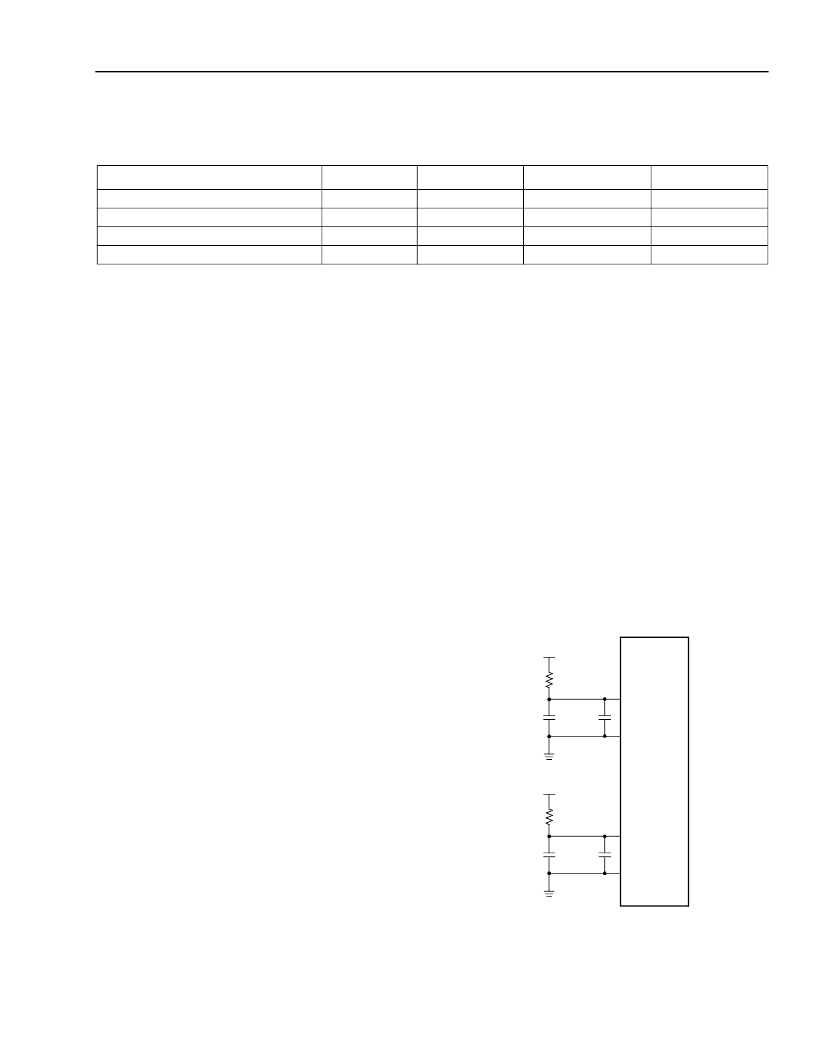
15.9 APLL V
DD
Filter
Separate V
DD
s
are provided for APLL1 and APLL2 for
filtering purposes. V
DD
filtering will provide stability in the
APLL, primarily the VCOs. An R/C low pass filter should
be applied to the PLL V
DD
s
, see Figure 62. Depending
on the quality of V
DD
and board layout characteristics,
the R/C values should be selected to filter out unwanted
frequencies above a targeted frequency. For example, a
25
resistor and 10
μ
F capacitor will have a cut-off
frequency of 636 Hz. Characterize the quality of your
V
DD
and select component values accordingly. 25
is
the maximum recommended resistor value. At high fre-
quencies the ESR of a bulk cap becomes a problem (no
longer effectively low passes) so a high-frequency cap of
0.1
μ
F or so is required to compensate for some of the
higher clocks and various harmonics. This needs to be
placed as close to the T8110 device as possible to mini-
mize the radiational pick-up in the remaining trace
length. APLL1 and APLL2 each draw approximately
7 mA at 3.3 V. Hot swap applications can use late power
to ensure the capacitance and in-rush current do not vio-
late the PICMG Hot Swap specification.
0995(F)
Figure 62. APLL V
DD
Filtering
V
SS
T8110
APLL1V
DD
V
SS
APLL2V
DD
V
DD
= 3.3 V
V
DD
= 3.3 V
R
C
R
C
0.1
μ
F
0.1
μ
F
相關(guān)PDF資料 |
PDF描述 |
|---|---|
| T8301 | T8301 Internet Protocol Telephone Phone-On-A-Chip⑩ IP Solution DSP |
| T8302 | T8302 Internet Protocol Telephone Advanced RISC Machine (ARM) Ethernet QoS Using IEEE 802.1q |
| T8502 | T8502 and T8503 Dual PCM Codecs with Filters |
| T8503 | T8502 and T8503 Dual PCM Codecs with Filters |
| T8531A | T8531A/8532 Multichannel Programmable Codec Chip Set |
相關(guān)代理商/技術(shù)參數(shù) |
參數(shù)描述 |
|---|---|
| T811004 | 制造商:E-SWITCH 制造商全稱:E-SWITCH 功能描述:E-SWITCH 800SP9B5M2QE |
| T-8110---BAL-DB | 制造商:LSI Corporation 功能描述:Switch Fabric 4K x 4K 3.3V 272-Pin BGA |
| T8110L | 制造商:AGERE 制造商全稱:AGERE 功能描述:Ambassador㈢ T8110L H.100/H.110 Switch |
| T-8110L | 制造商:AGERE 制造商全稱:AGERE 功能描述:Ambassador㈢ T8110L H.100/H.110 Switch |
| T81110 | 制造商:Allied Controls Incorporated 功能描述:Conn Relay Socket SKT 8 POS Solder Lug ST Panel Mount |
發(fā)布緊急采購,3分鐘左右您將得到回復(fù)。